SLVSAB3I May 2010 – January 2016 DRV8832
PRODUCTION DATA.
- 1 Features
- 2 Applications
- 3 Description
- 4 Revision History
- 5 Pin Configuration and Functions
- 6 Specifications
- 7 Detailed Description
- 8 Application and Implementation
- 9 Power Supply Recommendations
- 10Layout
- 11Device and Documentation Support
- 12Mechanical, Packaging, and Orderable Information
封装选项
机械数据 (封装 | 引脚)
散热焊盘机械数据 (封装 | 引脚)
订购信息
7 Detailed Description
7.1 Overview
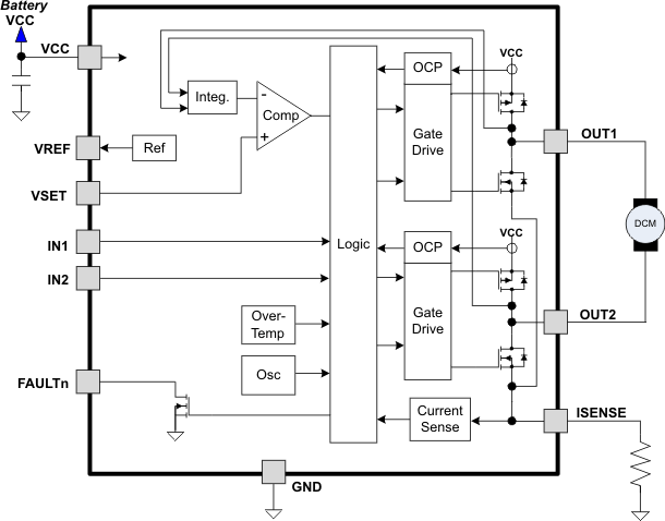
The DRV8832 is an integrated motor driver solution used for brushed motor control. The device integrates one H-bridge, current regulation circuitry, and a PWM voltage regulation method.
Using the PWM voltage regulation allows the motor to maintain the desired speed as VCC changes. Battery operation is an example of using this feature. When the battery is new or fully charged VCC will be higher than when the battery is old or partially discharged. The speed of the motor will vary based on the voltage of the battery. By setting the desired voltage across the motor at a lower voltage, a fully charged battery will use less power and spin the motor at the same speed as a battery that has been partially discharged.
7.2 Functional Block Diagram

7.3 Feature Description
7.3.1 PWM Motor Driver
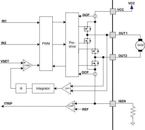
The DRV8832 contains an H-bridge motor driver with PWM voltage-control circuitry with current limit circuitry. Figure 7 shows a block diagram of the motor control circuitry.
 Figure 7. Motor Control Circuitry
7.3.2 Bridge Control
The IN1 and IN2 control pins enable the H-bridge outputs. Table 1 shows the logic:
Table 1. H-Bridge Logic
| IN1 | IN2 | OUT1 | OUT2 | Function |
|---|---|---|---|---|
| 0 | 0 | Z | Z | Sleep/Coast |
| 0 | 1 | L | H | Reverse |
| 1 | 0 | H | L | Forward |
| 1 | 1 | H | H | Brake |
When both inputs are low, the output drivers are disabled and the device is placed into a low-power sleep state. The current limit fault condition (if present) is also cleared. Note that when transitioning from either brake or sleep mode to forward or reverse, the voltage control PWM starts at zero duty cycle. The duty cycle slowly ramps up to the commanded voltage. This can take up to 12 ms to go from sleep to 100% duty cycle. Because of this, high-speed PWM signals cannot be applied to the IN1 and IN2 pins. To control motor speed, use the VSET pin as described below.
Because of the sleep mode functionality described previously, when applying an external PWM to the DRV8832, hold one input logic high while applying a PWM signal to the other. If the logic input is held low instead, then the device will cycle in and out of sleep mode, causing the FAULTn pin to pulse low on every sleep mode exit.
7.3.3 Voltage Regulation
The DRV8832 provides the ability to regulate the voltage applied to the motor winding. This feature allows constant motor speed to be maintained even when operating from a varying supply voltage such as a discharging battery.
The DRV8832 uses a pulse-width modulation (PWM) technique instead of a linear circuit to minimize current consumption and maximize battery life.
The circuit monitors the voltage difference between the output pins and integrates it, to get an average DC voltage value. This voltage is divided by 4 and compared to the VSET pin voltage. If the averaged output voltage (divided by 4) is lower than VSET, the duty cycle of the PWM output is increased; if the averaged output voltage (divided by 4) is higher than VSET, the duty cycle is decreased.
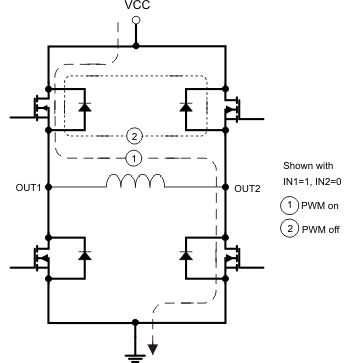
During PWM regulation, the H-bridge is enabled to drive current through the motor winding during the PWM on time. This is shown in the diagram below as case 1. The current flow direction shown indicates the state when IN1 is high and IN2 is low.
Note that if the programmed output voltage is greater than the supply voltage, the device will operate at 100% duty cycle and the voltage regulation feature will be disabled. In this mode the device behaves as a conventional H-bridge driver.
During the PWM off time, winding current is recirculated by enabling both of the high-side FETs in the bridge as shown in Figure 8.
 Figure 8. Voltage Regulation
7.3.4 Reference Output
The DRV8832 includes a reference voltage output that can be used to set the motor voltage. Typically for a constant-speed application, VSET is driven from VREF through a resistor divider to provide a voltage equal to 1/4 the desired motor drive voltage.
For example, if VREF is connected directly to VSET, the voltage will be regulated at 5.14 V. If the desired motor voltage is 3 V, VREF should be 0.75 V. This can be obtained with a voltage divider using 53 kΩ from VREF to VSET, and 75 kΩ from VSET to GND.
7.3.5 Current Limit
A current limit circuit is provided to protect the system in the event of an overcurrent condition, such as what would be encountered if driving a DC motor at start-up or with an abnormal mechanical load (stall condition).
The motor current is sensed by monitoring the voltage across an external sense resistor. When the voltage exceeds a reference voltage of 200 mV for more than approximately 3 µs, the PWM duty cycle is reduced to limit the current through the motor to this value. This current limit allows for starting the motor while controlling the current.
If the current limit condition persists for some time, it is likely that a fault condition has been encountered, such as the motor being run into a stop or a stalled condition. An overcurrent event must persist for approximately
275 ms before the fault is registered. After approximately 275 ms, a fault signaled to the host by driving the FAULTn signal low. Operation of the motor driver will continue.
The current limit fault condition is self-clearing and will be released when the abnormal load (stall condition) is removed.
The resistor used to set the current limit must be less than 1 Ω. Its value may be calculated using Equation 1:

where
- RISENSE is the current sense resistor value
- ILIMIT is the desired current limit (in mA)
If the current limit feature is not needed, the ISENSE pin may be directly connected to ground.
7.3.6 Protection Circuits
The DRV8832 is fully protected against undervoltage, overcurrent and overtemperature events.
7.3.6.1 Overcurrent Protection (OCP)
An analog current limit circuit on each FET limits the current through the FET by removing the gate drive. If this analog current limit persists for longer than the OCP time, all FETs in the H-bridge will be disabled, and the FAULTn signal will be driven low. The device will remain disabled until VCC is removed and re-applied.
Overcurrent conditions are sensed independently on both high and low side devices. A short to ground, supply, or across the motor winding will all result in an overcurrent shutdown. Note that OCP is independent of the current limit function, which is typically set to engage at a lower current level; the OCP function is intended to prevent damage to the device under abnormal (for example, short-circuit) conditions.
7.3.6.2 Thermal Shutdown (TSD)
If the die temperature exceeds safe limits, all FETs in the H-bridge will be disabled and the FAULTn signal will be driven low. Once the die temperature has fallen to a safe level operation will automatically resume.
7.3.6.3 Undervoltage Lockout (UVLO)
If at any time the voltage on the VCC pins falls below the undervoltage lockout threshold voltage, all circuitry in the device will be disabled, the FAULTn signal will be driven low, and internal logic will be reset. Operation will resume when VCC rises above the UVLO threshold.
Table 2. Device Protection
| FAULT | CONDITION | ERROR REPORT | H-BRIDGE | INTERNAL CIRCUITS | RECOVERY |
|---|---|---|---|---|---|
| VCC undervoltage (UVLO) | VCC < VUVLO | FAULTn | Disabled | Disabled | VCC > VUVLO |
| Overcurrent (OCP) | IOUT > IOCP | FAULTn | Disabled | Operating | Power Cycle VCC |
| Thermal Shutdown (TSD) | TJ > TTSD | FAULTn | Disabled | Operating | TJ < TTSD – THYS |
7.4 Device Functional Modes
The DRV8832 is active when either IN1 or IN2 are set to a logic high. Sleep mode is entered when both IN1 and IN2 are set to a logic low. When in sleep mode, the H-bridge FETs are disabled (Hi-Z).
Table 3. Modes of Operation
| FAULT | CONDITION | H-BRIDGE | INTERNAL CIRCUITS |
|---|---|---|---|
| Operating | IN1 or IN2 high | Operating | Operating |
| Sleep mode | IN1 and IN2 low | Disabled | Disabled |
| Fault encountered | Any fault condition met | Disabled | See Table 2 |