ZHCSDG6C March 2015 – January 2023 DRV2700
PRODUCTION DATA
- 1 特性
- 2 应用
- 3 说明
- 4 Revision History
- 5 Pin Configuration and Functions
- 6 Specifications
- 7 Detailed Description
-
8 Application and Implementation
- 8.1 Application Information
- 8.2
Typical Applications
- 8.2.1
AC-Coupled DAC Input Application
- 8.2.1.1 Design Requirements
- 8.2.1.2
Detailed Design Procedure
- 8.2.1.2.1 Piezo Load Selection
- 8.2.1.2.2 Programming The Boost Voltage
- 8.2.1.2.3 Inductor and Transformer Selection
- 8.2.1.2.4 Programing the Boost and Flyback Current-Limit
- 8.2.1.2.5 Boost Capacitor Selection
- 8.2.1.2.6 Pulldown FET and Resistors
- 8.2.1.2.7 Low-Voltage Operation
- 8.2.1.2.8 Current Consumption Calculation
- 8.2.1.2.9 Input Filter Considerations
- 8.2.1.2.10 Output Limiting Factors
- 8.2.1.2.11 Startup and Shutdown Sequencing
- 8.2.1.3 Application Curves
- 8.2.2 Filtered AC Coupled Single-Ended PWM Input Application
- 8.2.3 DC-Coupled DAC Input Application
- 8.2.4 DC-Coupled Reference Input Application
- 8.2.5 Flyback Circuit
- 8.2.1
AC-Coupled DAC Input Application
- 8.3 System Example
- 9 Power Supply Recommendations
- 10Layout
- 11Device and Documentation Support
- 12Mechanical, Packaging, and Orderable Information
封装选项
请参考 PDF 数据表获取器件具体的封装图。
机械数据 (封装 | 引脚)
- RGP|20
散热焊盘机械数据 (封装 | 引脚)
- RGP|20
订购信息
8.2.1.2.1 Piezo Load Selection
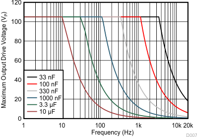
Several key specifications must be considered when selecting a piezo actuator such as dimensions, blocking force, and displacement. However, the key electrical specifications from the driver perspective are voltage rating and capacitance. The DRV2700 device operating in boost + amplifier mode can drive a variety of capacitances, frequencies, and voltages. However to extend the range in one specification can decrease the range of another specification. For example, if driving audio tones around 1 kHz, a lower capacitance piezo or lower driving voltage may be required. Figure 8-2 shows a general guide to selecting the proper parameters.
 Figure 8-2 Maximum Frequency versus Maximum Voltage for Different Load Capacitances
Based on the design example, if the output voltage must be ±60 VOUT to 2 kHz, then the piezo capacitance must be less than 100 nF. For ease of calculation, use a piezo load capacitance of 25 nF.