ZHCSA85F August   2012  – February 2019 DLPC410

PRODUCTION DATA.  

  1. 特性
  2. 应用
  3. 说明
    1.     Device Images
      1.      简化应用
  4. 修订历史记录
  5. 说明 (续)
  6. Pin Configuration and Functions
    1.     Pin Functions
  7. Specifications
    1. 7.1 Absolute Maximum Ratings
    2. 7.2 ESD Ratings
    3. 7.3 Recommended Operating Conditions
    4. 7.4 Electrical Characteristics
    5. 7.5 Timing Requirements
  8. Detailed Description
    1. 8.1 Overview
    2. 8.2 Functional Block Diagrams
    3. 8.3 Feature Description
      1. 8.3.1 DLPC410 Binary Pattern Data Path
        1. 8.3.1.1  DIN_A, DIN_B, DIN_C, DIN_D Input Data Buses
        2. 8.3.1.2  DCLKIN Input Clocks
        3. 8.3.1.3  DVALID Input Signals
        4. 8.3.1.4  DOUT_A, DOUT_B, DOUT_C, DOUT_D Output Data Buses
        5. 8.3.1.5  DCLKOUT Output Clocks
        6. 8.3.1.6  SCTRL Output Signals
        7. 8.3.1.7  Supported DMD Bus Sizes
        8. 8.3.1.8  Row Cycle definition
        9. 8.3.1.9  DLP9500 and DLP9500UV Input Data Formatting
        10. 8.3.1.10 DLP7000 and DLP7000UV Input Data Bus
        11. 8.3.1.11 DLP650LNIR Input Data Bus
      2. 8.3.2 Data Bus Operations
        1. 8.3.2.1 Row Addressing
        2. 8.3.2.2 Single Row Write Operation
        3. 8.3.2.3 No-Op Row Cycle Description
      3. 8.3.3 DMD Block Operations
        1. 8.3.3.1 Mirror Clocking Pulse (MCP)
        2. 8.3.3.2 Reset Active (RST_ACTIVE)
        3. 8.3.3.3 DMD Block Control Signals
          1. 8.3.3.3.1 Block Mode - BLK_MD1:0)
          2. 8.3.3.3.2 Block Address - BLK_AD(3:0)
          3. 8.3.3.3.3 Reset 2 Blocks - RST2BLK
        4. 8.3.3.4 DMD Block Operations
          1. 8.3.3.4.1 Global Reset (MCP) Consideration
      4. 8.3.4 Other Data Control Inputs
        1. 8.3.4.1 Complement Data
        2. 8.3.4.2 North/South Flip
      5. 8.3.5 Miscellaneous Control Inputs
        1. 8.3.5.1 ARST
        2. 8.3.5.2 CLKIN_R
        3. 8.3.5.3 DMD_A_RESET
        4. 8.3.5.4 Watchdog Timer Enable (WDT_ENABLE)
      6. 8.3.6 Miscellaneous Status Outputs
        1. 8.3.6.1 INIT_ACTIVE
        2. 8.3.6.2 DMD_Type(3:0)
        3. 8.3.6.3 DDC_VERSION(3:0)
        4. 8.3.6.4 LED0
        5. 8.3.6.5 LED1
        6. 8.3.6.6 DLPA200 Control Signals
        7. 8.3.6.7 ECM2M_TP_ (31:0)
    4. 8.4 Device Functional Modes
      1. 8.4.1 DLPC410 Initialization and Training
        1. 8.4.1.1 Initialization
        2. 8.4.1.2 input Data Interface (DIN) Training Pattern
      2. 8.4.2 DLPC410 Operational Modes
        1. 8.4.2.1 Single Block Mode
        2. 8.4.2.2 Single Block Phased Mode
        3. 8.4.2.3 Dual Block Mode
        4. 8.4.2.4 Quad Block Mode
        5. 8.4.2.5 Global Mode
        6. 8.4.2.6 DMD Park Mode
        7. 8.4.2.7 DMD Idle Mode
      3. 8.4.3 LOAD4 Functionality (enabled with DLPR410A)
        1. 8.4.3.1 Enabling LOAD4
        2. 8.4.3.2 Loading Data with LOAD4
        3. 8.4.3.3 Row Mapping with LOAD4
        4. 8.4.3.4 Using Block Clear with LOAD4
        5. 8.4.3.5 Timing Requirements for LOAD4
        6. 8.4.3.6 Global Binary Pattern Rate increases using LOAD4
        7. 8.4.3.7 Special LOAD4 considerations
    5. 8.5 Programming
  9. Application and Implementation
    1. 9.1 Application Information
      1. 9.1.1 Device Description
    2. 9.2 Typical Application
      1. 9.2.1 Design Requirements
      2. 9.2.2 Detailed Design Procedure
      3. 9.2.3 Application Curves
    3. 9.3 Initialization Setup
      1. 9.3.1 Debugging Guidelines
      2. 9.3.2 Initialization
        1. 9.3.2.1 Calibration
        2. 9.3.2.2 DLPA200 Number 1 Initialization
        3. 9.3.2.3 DMD Initialization
          1. 9.3.2.3.1 DMD Device ID Check
          2. 9.3.2.3.2 DMD Device OK
        4. 9.3.2.4 DLPA200 Number 2 Initialization
        5. 9.3.2.5 Command Sequence Initialization
      3. 9.3.3 Image Display Issues
        1. 9.3.3.1 Present Data to DLPC410
        2. 9.3.3.2 Load Data to DMD
        3. 9.3.3.3 Mirror Clocking Pulse
  10. 10Power Supply Recommendations
    1. 10.1 Power Down Operation
  11. 11Layout
    1. 11.1 Layout Guidelines
      1. 11.1.1 Impedance Requirements
      2. 11.1.2 PCB Signal Routing
      3. 11.1.3 Fiducials
      4. 11.1.4 PCB Layout Guidelines
        1. 11.1.4.1 DMD Interface
          1. 11.1.4.1.1 Trace Length Matching
        2. 11.1.4.2 DLPC410 DMD Decoupling
          1. 11.1.4.2.1 Decoupling Capacitors
        3. 11.1.4.3 VCC and VCC2
        4. 11.1.4.4 DMD Layout
        5. 11.1.4.5 DLPA200
    2. 11.2 Layout Example
    3. 11.3 DLPC410 Chipset Connections
  12. 12器件和文档支持
    1. 12.1 器件支持
      1. 12.1.1 器件标记
      2. 12.1.2 器件命名规则
    2. 12.2 文档支持
      1. 12.2.1 相关文档
    3. 12.3 社区资源
    4. 12.4 商标
    5. 12.5 静电放电警告
    6. 12.6 术语表
  13. 13机械、封装和可订购信息

封装选项

机械数据 (封装 | 引脚)
  • DLP|676
散热焊盘机械数据 (封装 | 引脚)
订购信息

input Data Interface (DIN) Training Pattern

The DLPC410 detects the phase differences between the ½ speed clock (used in the customer device driving the LVDS data) and the internally generated ½ speed data clocks and automatically corrects their alignment. This is done by the customer FPGA supplying a simple repeating pattern on all of the data inputs while the INIT_ACTIVE output of the DLPC410 is high/active. The details of the training pattern are described below.

This is a simple block diagram of the training pattern insertion logic.
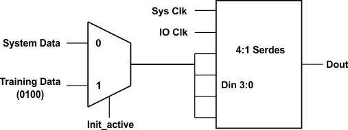
DLPC410 blk_dia_logic_lps024.gifFigure 12. Block Diagram of Training Pattern Logic

The expected training pattern is 0100. In Figure 13 the data input to the 4:1 SERDES cells is captured on the rising edge of the ½ speed system clock. The output latency shown is based on the documentation for the Xilinx SERDES cells. Individual implementation may vary depending on the type of cells, technology, and design technique used.
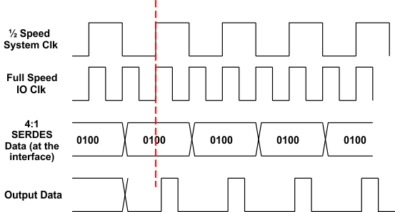
DLPC410 patt_align_lps024.gifFigure 13. Training Pattern Alignment

NOTE

In Xilinx FPGAs (due to the construction of the ISERDES and OSERDES cells) a pattern of 0010 needs to be applied to the output/transmitting SERDES cells data pins (D1 = 0, D2 = 0, D3 = 1, D4 = 0) in order to receive a result of 0100 (Q1 = 0, Q2 = 1, Q3 = 0, Q4 = 0) at the input/receiving SERDES cell.

The patterns should be applied on all of the input data and DVALID pins. In this respect, the interface is treated as a 17 bit interface with DVALID being the 17th data bit. The receiving logic in the DLPC410 will shift the data until the correct pattern is seen at the inputs. The SERDES cells align the incoming data with the ½ speed system clock (derived from the full speed data clock). This allows DLPC410 to correctly align the DVALID signal and the incoming data and will contribute to a more robust interface. It is important that the training pattern is applied to the DVALID and data inputs of the DLPC410 before reset to the device is deasserted, as training commences immediately on the deassertion of reset. The INIT_ACTIVE signal is asserted while the device is held in reset in order to help facilitate this behavior.