ZHCSAV5F April 2013 – May 2019 DLPC350
PRODUCTION DATA.
- 1 特性
- 2 应用
- 3 说明
- 4 修订历史记录
- 5 Pin Configuration and Functions
-
6 Specifications
- 6.1 Absolute Maximum Ratings
- 6.2 ESD Ratings
- 6.3 Recommended Operating Conditions
- 6.4 Thermal Information
- 6.5 I/O Electrical Characteristics
- 6.6 I2C0 and I2C1 Interface Timing Requirements
- 6.7 Port 1 Input Pixel Interface Timing Requirements
- 6.8 Port 2 Input Pixel Interface (FPD-Link Compatible LVDS Input) Timing Requirements
- 6.9 System Oscillator Timing Requirements
- 6.10 Reset Timing Requirements
- 6.11 Video Timing Input Blanking Specification
- 6.12 Programmable Output Clocks Switching Characteristics
- 6.13 DMD Interface Switching Characteristics
- 6.14 JTAG Interface: I/O Boundary Scan Application Switching Characteristics
- 7 Parameter Measurement Information
- 8 Detailed Description
- 9 Application and Implementation
- 10Power Supply Recommendations
-
11Layout
- 11.1 Layout Guidelines
- 11.2 Layout Example
- 12器件和文档支持
- 13机械、封装和可订购信息
8.4.1 Structured Light Applications
For applications where video enhancement is not desired, the video processing algorithms can be bypassed and replaced with a specific set of bit-planes. The pattern image is then allocated into the corresponding time slots. Furthermore, an output trigger signal is synchronized with these time slots to indicate when the image is displayed. For structured light applications, this mechanism provides the capability to display a set of patterns and signal a camera to capture these patterns overlaid on an object.
The DLPC350 controller stores two 24-bit frames in its internal memory buffer. This display buffer, composed of 48 1-bit planes, allows the DLPC350 controller to send one 24-bit buffer to the DMD array while the second 24-bit buffer is filled from the flash or streamed in through the 24-bit RGB interface. In streaming mode, the DMD array displays the previous 24-bit frame while the current 24-bit frame fills the second display buffer. After a 24-bit frame is displayed, the buffer rotates, accessing the next 24-bit frame to the DMD. Thus, the displayed image is a 24-bit frame behind the data streamed through the 24-bit RGB parallel interface.
In structured light mode, the maximum pattern rate can be achieved by pre-loading the 48 1-bit planes from flash memory, and sequencing them in the desired order with different bit depths. In order to achieve this maximum pre-loaded pattern rate shown in Table 8, it is required to display all the patterns from one 24-bit frame buffer before displaying patterns from the second 24-bit frame buffer. If all displayed patterns cannot fit inside the 48 1-bit plane buffer, the maximum pattern rate cannot be achieved as a load penalty will be incurred when loading one side of the buffer as the other is displayed. To synchronize a camera to the displayed patterns, the DLPC350 controller supports three trigger modes: mode 0, mode 1, and mode 2. An overview of the modes can be found in Table 7.
Table 7. Trigger Modes
| TRIG_IN_1 | TRIG_IN_2 | TRIG_OUT_1 | TRIG_OUT_2 | |
|---|---|---|---|---|
| Mode 0 | Unused (uses VSYNC) | Starts and stops pattern sequence | Asserted during exposure time | Start of the pattern sequence |
| Mode 1 | Advances to next pattern | Starts and stops pattern sequence | Asserted during exposure time | Start of the pattern sequence |
| Mode 2 | Alternates between two patterns | Advances to next pair of patterns | Asserted during exposure time | Start of the pattern sequence |
In mode 0, the vertical sync (VSYNC) acts as the trigger input (TRIG_IN_1 is unused), and TRIG_IN_2 starts and stops the pattern sequence on the rising and falling edge respectively. In mode 1, a TRIG_IN_1 pulse indicates to the DLPC350 controller to advance to the next pattern, while TRIG_IN_2 starts and stops the pattern sequence on the rising and falling edge respectively. In mode 2, the TRIG_IN_1 signal toggles between two consecutive patterns, while a TRIG_IN_2 pulse advances to the next pair of patterns. In all modes, TRIG_OUT_1 is asserted during the exposure time of the pattern, while TRIG_OUT_2 pulses at the start of the pattern sequence .
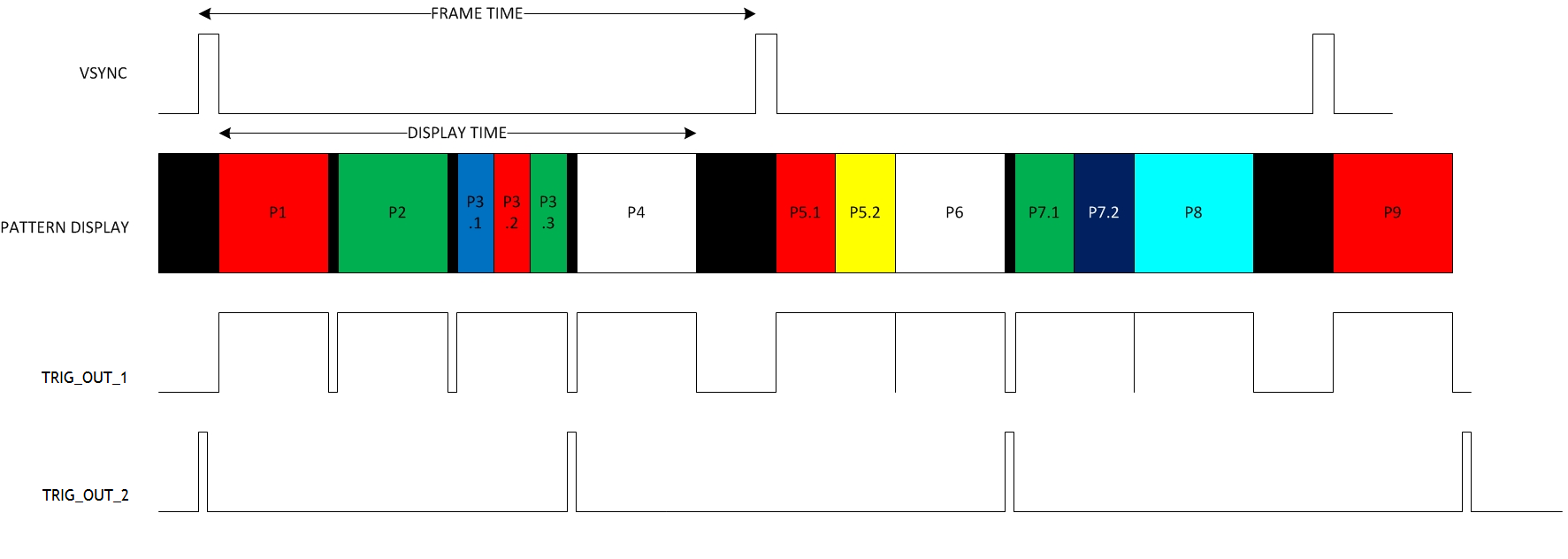
An example of mode 0 is shown in Figure 15, where the VSYNC signal starts the pattern sequence display. The pattern sequence consists of a series of three consecutive patterns. The first pattern sequence consists of P1, P2, and P3. Because P3 is an RGB pattern, it is shown with its time sequential representation of P3.1, P3.2, and P3.3. The second pattern sequence consists of three patterns: P4, P5, and P6. The third sequence consists of P7, P8, and P9. TRIG_OUT_1 is high for each pattern exposure period, while TRIG_OUT_2 indicates the start of each of the three pattern sequences.
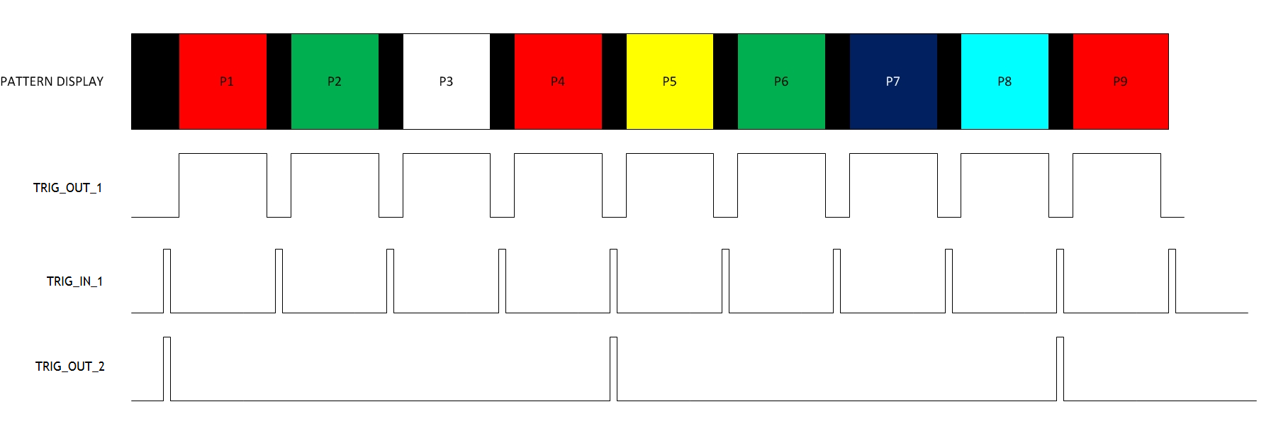
An example of mode 1 is shown in Figure 16, where pattern sequences of four are displayed. TRIG_OUT_1 is asserted for each pattern exposure period, while TRIG_OUT_2 indicates the start of each four-pattern sequence. TRIG_IN_1 pulses advance the pattern.
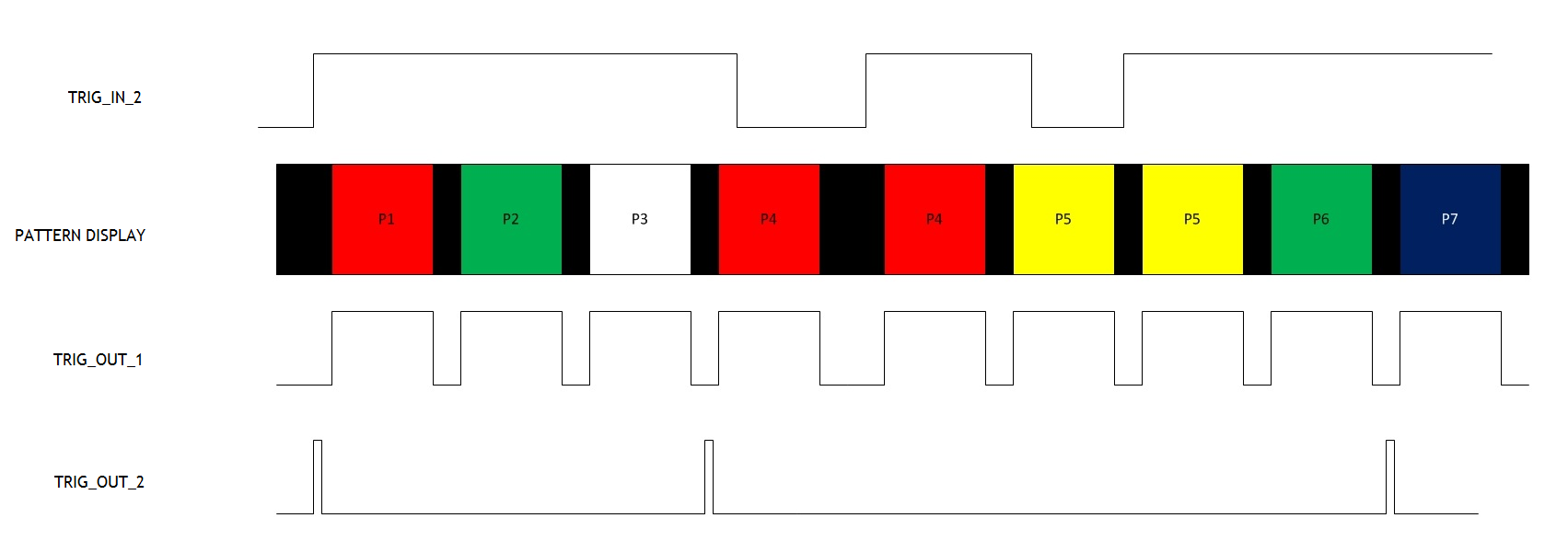
Another example of mode 1 is shown in Figure 17, where pattern sequences of three are displayed. TRIG_OUT_1 is asserted during each pattern exposure, while TRIG_OUT_2 indicates the start of each three-pattern sequence. TRIG_IN_2 serves as a start and stop signal. When high, the pattern sequence starts or continues. Note that in the middle of displaying the P4 pattern, TRIG_IN_2 is low, so the sequence stops displaying P4. When TRIG_IN_2 is raised, the pattern sequence continues where it stopped by re-displaying P4.
An example of mode 2 is shown in Figure 18, where TRIG_IN_1 alternates between two patterns, while TRIG_IN_2 advances to the next pair of patterns.
 Figure 15. Mode 0 Trigger Timing Diagram
  Figure 16. Mode 1 Triggers Timing Diagram for 6-bit Patterns
  Figure 17. Mode 1 Trigger Timing Diagram
  Figure 18. Mode 2 Trigger Timing Diagram
 Table 8. Allowed Pattern Combinations
| BIT DEPTH | EXTERNAL RGB INPUT PATTERN RATE (Hz) | PRE-LOADED PATTERN RATE (Hz) | MAXIMUM NUMBER OF PATTERNS
(PRE-LOADED) |
|---|---|---|---|
| 1 | 2880 | 4225 | 48 |
| 2 | 1428 | 1428 | 24 |
| 3 | 636 | 636 | 16 |
| 4 | 588 | 588 | 12 |
| 5 | 480 | 500 | 8 |
| 6 | 400 | 400 | 8 |
| 7 | 222 | 222 | 6 |
| 8 | 120 | 120 | 6 |