ZHCSD21 October 2014 DLP6500FLQ
PRODUCTION DATA.
- 1 特性
- 2 应用
- 3 说明
- 4 修订历史记录
- 5 Pin Configuration and Functions
-
6 Specifications
- 6.1 Absolute Maximum Ratings
- 6.2 Handling Ratings
- 6.3 Recommended Operating Conditions
- 6.4 Thermal Information
- 6.5 Electrical Characteristics
- 6.6 Timing Requirements
- 6.7 Typical Characteristics
- 6.8 System Mounting Interface Loads
- 6.9 Micromirror Array Physical Characteristics
- 6.10 Micromirror Array Optical Characteristics
- 6.11 Window Characteristics
- 6.12 Chipset Component Usage Specification
- 7 Detailed Description
- 8 Application and Implementation
- 9 Power Supply Recommendations
- 10Layout
- 11器件和文档支持
- 12机械封装和可订购信息
9 Power Supply Recommendations
9.1 DMD Power Supply Requirements
The following power supplies are all required to operate the DMD: VCC, VCCI, VOFFSET, VBIAS, and VRESET. VSS must also be connected. DMD power-up and power-down sequencing is strictly controlled by the DLPC900 device.
CAUTION
For reliable operation of the DMD, the following power supply sequencing requirements must be followed. Failure to adhere to the prescribed power-up and power-down procedures may affect device reliability. VCC, VCCI, VOFFSET, VBIAS, and VRESET power supplies have to be coordinated during power-up and power-down operations. VSS must also be connected. Failure to meet any of the below requirements will result in a significant reduction in the DMD’s reliability and lifetime. Refer to Figure 17.
9.2 DMD Power Supply Power-Up Procedure
- During power-up, VCC and VCCI must always start and settle before VOFFSET, VBIAS, and VRESET voltages are applied to the DMD.
- During power-up, it is a strict requirement that the delta between VBIAS and VOFFSET must be within the specified limit shown in Recommended Operating Conditions . During power-up, VBIAS does not have to start after VOFFSET.
- During power-up, there is no requirement for the relative timing of VRESET with respect to VOFFSET and VBIAS.
- Power supply slew rates during power-up are flexible, provided that the transient voltage levels follow the requirements listed in Absolute Maximum Ratings , in Recommended Operating Conditions, and in Figure 17.
- During power-up, LVCMOS input pins shall not be driven high until after VCC and VCCI have settled at operating voltages listed in Recommended Operating Conditions.
9.3 DMD Power Supply Power-Down Procedure
- During power-down, VCC and VCCI must be supplied until after VBIAS, VRESET, and VOFFSET are discharged to within the specified limit of ground. Refer to Table 4.
- During power-down, it is a strict requirement that the delta between VBIAS and VOFFSET must be within the specified limit shown in Recommended Operating Conditions. During power-down, it is not mandatory to stop driving VBIAS prior to VOFFSET.
- During power-down, there is no requirement for the relative timing of VRESET with respect to VOFFSET and VBIAS.
- Power supply slew rates during power-down are flexible, provided that the transient voltage levels follow the requirements listed in Absolute Maximum Ratings, in Recommended Operating Conditions , and in Figure 17.
- During power-down, LVCMOS input pins must be less than specified in Recommended Operating Conditions.
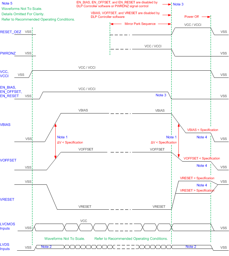 Figure 17. DMD Power Supply Sequencing Requirements
- To prevent excess current, the supply voltage delta |VBIAS – VOFFSET| must be less than specified in Recommended Operating Conditions. OEMs may find that the most reliable way to ensure this is to power VOFFSET prior to VBIAS during power-up and to remove VBIAS prior to VOFFSET during power-down.
- LVDS signals are less than the input differential voltage (VID) maximum specified in Recommended Operating Conditions. During power-down, LVDS signals are less than the high level input voltage (VIH) maximum specified in Recommended Operating Conditions.
- When system power is interrupted, the DLP controller (DLPC900) initiates a hardware power-down that activates PWRDNZ and disables VBIAS, VRESET and VOFFSET after the micromirror park sequence. Software power-down disables VBIAS, VRESET, and VOFFSET after the micromirror park sequence through software control. For either case, enable signals EN_BIAS, EN_OFFSET, and EN_RESET are used to disable VBIAS, VOFFSET, and VRESET, respectfully.
- Refer to DMD Power Down Sequence Requirements.
- Figure not to scale. Details have been omitted for clarity. Refer Recommended Operating Conditions.
Table 4. DMD Power-Down Sequence Requirements
| PARAMETER | MIN | MAX | UNIT | |
|---|---|---|---|---|
| VBIAS | Supply voltage level during power–down sequence | 4.0 | V | |
| VOFFSET | Supply voltage level during power–down sequence | 4.0 | V | |
| VRESET | Supply voltage level during power–down sequence | –4.0 | 0.5 | V |