ZHCSG81 April 2017 DCPA10505 , DCPA10505D , DCPA10512 , DCPA10512D , DCPA10515 , DCPA10515D
PRODUCTION DATA.
- 1 特性
- 2 应用
- 3 说明
- 4 修订历史记录
- 5 Pin Configuration and Functions
-
6 Specifications
- 6.1 Absolute Maximum Ratings
- 6.2 ESD Ratings
- 6.3 Recommended Operating Conditions
- 6.4 Electrical Characteristics
- 6.5 Switching Characteristics
- 6.6 Typical Characteristics (DCPA10505)
- 6.7 Typical Characteristics (DCPA10512)
- 6.8 Typical Characteristics (DCPA10515)
- 6.9 Typical Characteristics (DCPA10505D)
- 6.10 Typical Characteristics (DCPA10512D)
- 6.11 Typical Characteristics (DCPA10515D)
-
7 Detailed Description
- 7.1 Overview
- 7.2 Functional Block Diagrams
- 7.3 Feature Description
- 8 Application and Implementation
- 9 Power Supply Recommendations
- 10Layout
- 11器件和文档支持
- 12机械、封装和可订购信息
8 Application and Implementation
NOTE
Information in the following applications sections is not part of the TI component specification, and TI does not warrant its accuracy or completeness. TI’s customers are responsible for determining suitability of components for their purposes. Customers should validate and test their design implementation to confirm system functionality.
8.1 Application Information
8.1.1 Ripple Reduction
The high switching frequency of 425 kHz allows simple filtering. To reduce output voltage ripple, it is recommended that a minimum of 1-µF capacitor be used on the +VOUT pin. For dual output devices, decouple both of the outputs to the COM pin. The required 2.2-µF, low ESR ceramic input capacitor also helps to reduce ripple and noise. See DC-to-DC Converter Noise Reduction (SBVA012).
8.1.2 Connecting the DCPA1 in Series
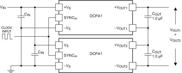
Multiple DCPA1 isolated 1-W DC/DC converters can be connected in series to provide non-standard voltage rails. This configuration is possible by using the floating outputs provided by the galvanic isolation of the DCPA1 devices by connecting the +VOUT from one DCPA1 to the –VOUT of another as shown in Figure 34. The synchronization feature allows easy synchronization to prevent power-rail beat frequencies at no additional filtering cost.
 Figure 34. Multiple DCPA1 Devices Connected in Series
The outputs of a dual-output DCPA1 device can also be connected in series to provide two times the magnitude of +VOUT, as shown in Figure 35. For example, connect a dual-output, ±15-V, DCPA10515D device to provide a 30-V rail.
 Figure 35. Dual Output Devices Connected in Series
8.1.3 Connecting the DCPA1 in Parallel
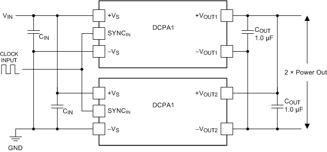
If the output power from one DCPA1 is not sufficient, it is possible to parallel the outputs of multiple DCPA1s, as shown in Figure 36, (applies to single output devices only). The synchronization feature allows easy synchronization to prevent power-rail beat frequencies at no additional filtering cost.
 Figure 36. Multiple DCPA1 Devices Connected in Parallel
8.2 Typical Application
 Figure 37. Typical DCPA10505 Application
8.2.1 Design Requirements
For this design example, use the parameters listed in Table 1 and follow the design procedures shown in Detailed Design Procedure section.
Table 1. Design Example Parameters
| PARAMETER | VALUE | UNIT | |
|---|---|---|---|
| V(+VS) | Input voltage | 5 | V |
| V(+VOUT) | Output voltage | 5 | V |
| IOUT | Output current rating | 200 | mA |
| fSW | Operating frequency | 425 | kHz |
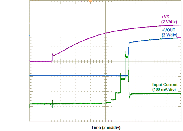
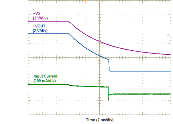
8.2.2 DCPA10505 Application Curves
 Figure 38. DCPA10505 Turn-ON
 Figure 39. DCPA10505 Turn-OFF
8.2.3 Detailed Design Procedure
8.2.3.1 Input Capacitor
For all DCPA1, 5-V input voltage designs, select a 2.2-μF low-ESR ceramic input capacitor to ensure a good startup performance.
8.2.3.2 Output Capacitor
For any DCPA1 design, select a 1.0-μF low-ESR ceramic output capacitor to reduce output ripple.
8.2.3.3 SYNCIN Pin
In a stand-alone application, it is recommended to connect this pin to the input side common, –VS.
8.2.4 PCB Design
The copper losses (resistance and inductance) can be minimized by the use of mutual ground and power planes where possible. If that is not possible, use wide traces to reduce the losses. If several devices are being powered from a common power source, a star-connected system for the traces must be deployed. Do not connect the devices in series, because that type of connection cascades the resistive losses. The position of the decoupling capacitors is important. They must be as close to the devices as possible in order to reduce losses. See the PCB Layout section for more details.