ZHCSEB0D September 2015 – July 2018 CC1310
PRODUCTION DATA.
- 1器件概述
- 2修订历史记录
- 3Device Comparison
- 4Terminal Configuration and Functions
-
5Specifications
- 5.1 Absolute Maximum Ratings
- 5.2 ESD Ratings
- 5.3 Recommended Operating Conditions
- 5.4 Power Consumption Summary
- 5.5 RF Characteristics
- 5.6 Receive (RX) Parameters, 861 MHz to 1054 MHz
- 5.7 Receive (RX) Parameters, 431 MHz to 527 MHz
- 5.8 Transmit (TX) Parameters, 861 MHz to 1054 MHz
- 5.9 Transmit (TX) Parameters, 431 MHz to 527 MHz
- 5.10 PLL Parameters
- 5.11 ADC Characteristics
- 5.12 Temperature Sensor
- 5.13 Battery Monitor
- 5.14 Continuous Time Comparator
- 5.15 Low-Power Clocked Comparator
- 5.16 Programmable Current Source
- 5.17 DC Characteristics
- 5.18 Thermal Characteristics
- 5.19 Timing and Switching Characteristics
- 5.20 Typical Characteristics
- 6Detailed Description
- 7Application, Implementation, and Layout
- 8器件和文档支持
- 9机械、封装和可订购信息
封装选项
机械数据 (封装 | 引脚)
散热焊盘机械数据 (封装 | 引脚)
订购信息
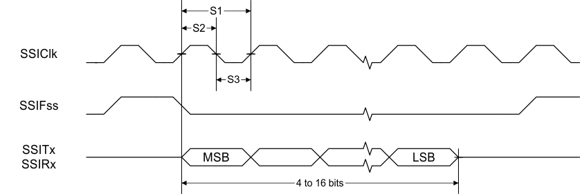
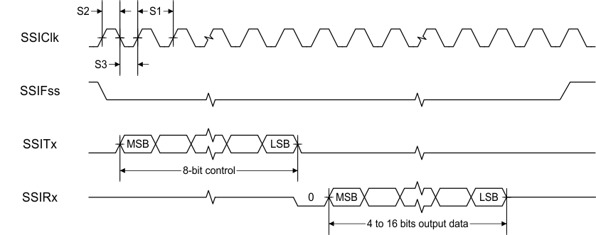
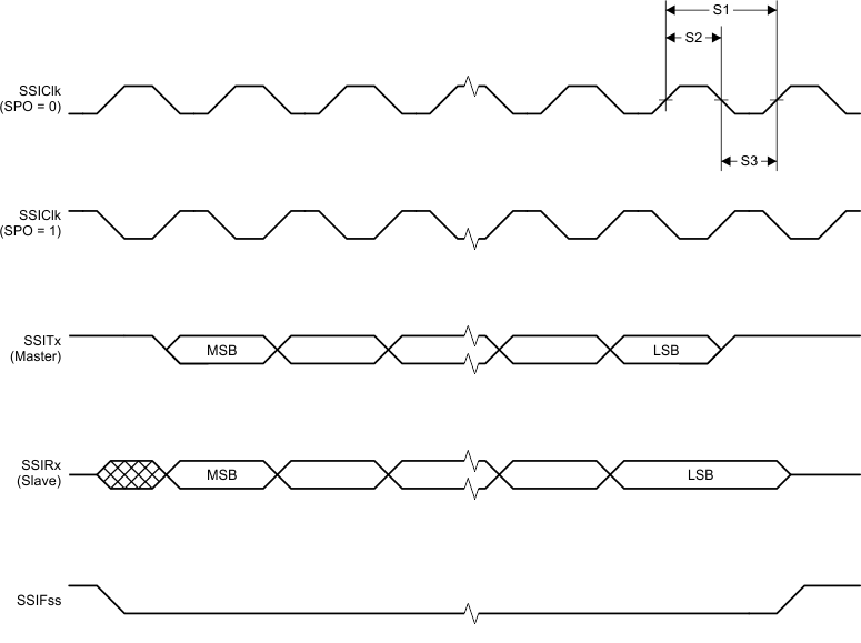
Table 5-8 Synchronous Serial Interface (SSI) Characteristics
Tc = 25°C, VDDS = 3.0 V, unless otherwise noted.| PARAMETER
NO. |
PARAMETER | MIN | TYP | MAX | UNIT | |
|---|---|---|---|---|---|---|
| S1 | tclk_per | SSIClk cycle time | 12 | 65024 | system clocks | |
| S2(1) | tclk_high | SSIClk high time | 0.5 × tclk_per | |||
| S3(1) | tclk_low | SSIClk low time | 0.5 × tclk_per | |||
 Figure 5-1 SSI Timing for TI Frame Format (FRF = 01), Single Transfer Timing Measurement
  Figure 5-2 SSI Timing for MICROWIRE Frame Format (FRF = 10), Single Transfer
  Figure 5-3 SSI Timing for SPI Frame Format (FRF = 00), With SPH = 1