SWRS108B May   2011  – June 2014 CC113L

PRODUCTION DATA.  

  1. 1Device Overview
    1. 1.1 Features
    2. 1.2 Applications
    3. 1.3 Description
    4. 1.4 Functional Block Diagram
  2. 2Revision History
  3. 3Terminal Configuration and Functions
    1. 3.1 Pin Diagram
    2. 3.2 Signal Descriptions
  4. 4Specifications
    1. 4.1  Absolute Maximum Ratings
    2. 4.2  Handling Ratings
    3. 4.3  Recommended Operating Conditions
    4. 4.4  General Characteristics
    5. 4.5  Current Consumption
      1. 4.5.1 Typical RX Current Consumption over Temperature and Input Power Level, 868/915 MHz
    6. 4.6  RF Receive Section
      1. 4.6.1 Typical Sensitivity over Temperature and Supply Voltage, 868 MHz, Sensitivity Optimized Setting
      2. 4.6.2 Typical Sensitivity over Temperature and Supply Voltage, 915 MHz, Sensitivity Optimized Setting
      3. 4.6.3 Blocking and Selectivity
    7. 4.7  Crystal Oscillator
    8. 4.8  Frequency Synthesizer Characteristics
    9. 4.9  DC Characteristics
    10. 4.10 Power-On Reset
    11. 4.11 Thermal Characteristics
    12. 4.12 Typical Characteristics
      1. 4.12.1 Typical Characteristics, RX Current Consumption
      2. 4.12.2 Typical Characteristics, Blocking and Selectivity
  5. 5Detailed Description
    1. 5.1  Overview
    2. 5.2  Functional Block Diagram
    3. 5.3  Configuration Overview
    4. 5.4  Configuration Software
    5. 5.5  4-wire Serial Configuration and Data Interface
      1. 5.5.1 Chip Status Byte
      2. 5.5.2 Register Access
      3. 5.5.3 SPI Read
      4. 5.5.4 Command Strobes
      5. 5.5.5 RX FIFO Access
    6. 5.6  Microcontroller Interface and Pin Configuration
      1. 5.6.1 Configuration Interface
      2. 5.6.2 General Control and Status Pins
    7. 5.7  Data Rate Programming
    8. 5.8  Receiver Channel Filter Bandwidth
    9. 5.9  Demodulator, Symbol Synchronizer, and Data Decision
      1. 5.9.1 Frequency Offset Compensation
      2. 5.9.2 Bit Synchronization
      3. 5.9.3 Byte Synchronization
    10. 5.10 Packet Handling Hardware Support
      1. 5.10.1 Packet Format
        1. 5.10.1.1 Arbitrary Length Field Configuration
        2. 5.10.1.2 Packet Length > 255
      2. 5.10.2 Packet Filtering
        1. 5.10.2.1 Address Filtering
        2. 5.10.2.2 Maximum Length Filtering
        3. 5.10.2.3 CRC Filtering
      3. 5.10.3 Packet Handling in Receive Mode
      4. 5.10.4 Packet Handling in Firmware
    11. 5.11 Modulation Formats
      1. 5.11.1 Frequency Shift Keying
      2. 5.11.2 Amplitude Modulation
    12. 5.12 Received Signal Qualifiers and RSSI
      1. 5.12.1 Sync Word Qualifier
      2. 5.12.2 RSSI
      3. 5.12.3 Carrier Sense (CS)
        1. 5.12.3.1 CS Absolute Threshold
        2. 5.12.3.2 CS Relative Threshold
    13. 5.13 Radio Control
      1. 5.13.1 Power-On Start-Up Sequence
        1. 5.13.1.1 Automatic POR
        2. 5.13.1.2 Manual Reset
      2. 5.13.2 Crystal Control
      3. 5.13.3 Voltage Regulator Control
      4. 5.13.4 Receive Mode (RX)
      5. 5.13.5 RX Termination
      6. 5.13.6 Timing
        1. 5.13.6.1 Overall State Transition Times
        2. 5.13.6.2 Frequency Synthesizer Calibration Time
    14. 5.14 RX FIFO
    15. 5.15 Frequency Programming
    16. 5.16 VCO
      1. 5.16.1 VCO and PLL Self-Calibration
    17. 5.17 Voltage Regulators
    18. 5.18 General Purpose and Test Output Control Pins
    19. 5.19 Asynchronous and Synchronous Serial Operation
      1. 5.19.1 Asynchronous Serial Operation
      2. 5.19.2 Synchronous Serial Operation
    20. 5.20 System Consideration and Guidelines
      1. 5.20.1 SRD Regulations
      2. 5.20.2 Calibration in Multi-Channel Systems
    21. 5.21 Configuration Registers
      1. 5.21.1 Configuration Register Details - Registers with preserved values in SLEEP state
      2. 5.21.2 Configuration Register Details - Registers that Loose Programming in SLEEP State
      3. 5.21.3 Status Register Details
    22. 5.22 Development Kit Ordering Information
  6. 6Applications, Implementation, and Layout
    1. 6.1 Bias Resistor
    2. 6.2 Balun and RF Matching
      1. 6.2.1 Balun and RF Matching (Low-Cost Application Circuit)
      2. 6.2.2 Balun and RF Matching (Characterization Circuit)
    3. 6.3 Crystal
    4. 6.4 Reference Signal
    5. 6.5 Power Supply Decoupling
    6. 6.6 PCB Layout Recommendations
  7. 7Device and Documentation Support
    1. 7.1 Device Support
      1. 7.1.1 Device Nomenclature
    2. 7.2 Documentation Support
      1. 7.2.1 Related Documentation from Texas Instruments
      2. 7.2.2 Community Resources
    3. 7.3 Trademarks
    4. 7.4 Electrostatic Discharge Caution
    5. 7.5 Export Control Notice
    6. 7.6 Glossary
    7. 7.7 Additional Acronyms
  8. 8Mechanical Packaging and Orderable Information
    1. 8.1 Packaging Information

封装选项

机械数据 (封装 | 引脚)
散热焊盘机械数据 (封装 | 引脚)
订购信息

1 Device Overview

1.1 Features

  • RF Performance
    • Receive Sensitivity Down to −116 dBm at
      0.6 kbps
    • Programmable Data Rate from 0.6 to 600 kbps
    • Frequency Bands: 300–348 MHz,
      387–464 MHz, and 779–928 MHz
    • 2-FSK, 4-FSK, GFSK, MSK, and OOK Supported
  • Digital Features
    • Flexible Support for Packet Oriented Systems
    • On-chip Support for Sync Word Detection, Flexible Packet Length, and Automatic CRC Calculation
  • Low-Power Features
    • 200-nA Sleep Mode Current Consumption
    • Fast Startup Time; 240 μs From Sleep to RX Mode
    • 64-Byte RX FIFO
  • General
    • Few External Components; Completely On-chip Frequency Synthesizer, No External Filters or RF Switch Needed
    • Green Package: RoHS Compliant and No Antimony or Bromine
    • Small Size (QLP 4- x 4-mm Package, 20 Pins)
    • Suited for Systems Targeting Compliance with EN 300 220 (Europe) and FCC CFR Part 15 (US)
    • Support for Asynchronous and Synchronous Serial Transmit Mode for Backward Compatibility with Existing Radio Communication Protocols

1.2 Applications

  • Ultra Low-Power Wireless Applications Operating in the 315-, 433-, 868-, 915-MHz ISM or SRD Bands
  • Wireless Alarm and Security Systems
  • Industrial Monitoring and Control
  • Remote Controls
  • Toys
  • Home and Building Automation

1.3 Description

The CC113L is a cost optimized sub-1 GHz RF receiver for the 300–348 MHz, 387–464 MHz, and 779–928 MHz frequency bands. The circuit is based on the popular CC1101 RF transceiver, and RF performance characteristics are identical. The CC115L transmitter together with the CC113L receiver enable a low-cost RF link.

The RF receiver is integrated with a highly configurable baseband demodulator. The modem supports various modulation formats and has a configurable data rate up to 600 kbps.

The CC113L provides extensive hardware support for packet handling, data buffering, and burst transmissions.

The main operating parameters and the 64-byte receive FIFO of CC113L can be controlled through a serial peripheral interface (SPI). In a typical system, the CC113L will be used together with a microcontroller and a few additional passive components.

Device Information(1)

PART NUMBER PACKAGE BODY SIZE
CC113LRGP QFN (20) 4.00 mm × 4.00 mm
(1) For more information on these devices, see Section 8, Mechanical Packaging and Orderable Information.

1.4 Functional Block Diagram

Figure 1-1 shows a functional block diagram of the device.

CC110L_simp_bd_swrs108.gif
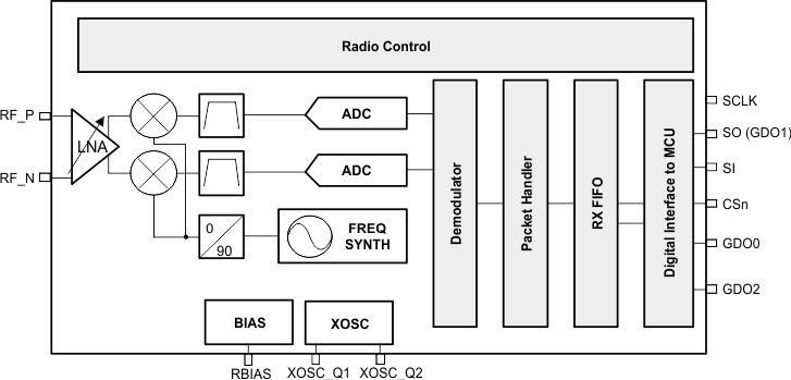
Figure 1-1 Functional Block Diagram