SWRS112H June 2011 – July 2015 CC1120
PRODUCTION DATA.
- 1Device Overview
- 2Revision History
- 3Terminal Configuration and Functions
-
4Specifications
- 4.1 ESD Ratings
- 4.2 Recommended Operating Conditions (General Characteristics)
- 4.3 RF Characteristics
- 4.4 Power Consumption Summary
- 4.5 Receive Parameters
- 4.6 Transmit Parameters
- 4.7 PLL Parameters
- 4.8 32-MHz Clock Input (TCXO)
- 4.9 32-MHz Crystal Oscillator
- 4.10 32-kHz Clock Input
- 4.11 32-kHz RC Oscillator
- 4.12 I/O and Reset
- 4.13 Temperature Sensor
- 4.14 Thermal Resistance Characteristics for RHB Package
- 4.15 Timing Requirements
- 4.16 Regulatory Standards
- 4.17 Typical Characteristics
- 5Detailed Description
- 6Application, Implementation, and Layout
- 7Device and Documentation Support
- 8Mechanical Packaging and Orderable Information
6 Application, Implementation, and Layout
NOTE
Information in the following Applications section is not part of the TI component specification, and TI does not warrant its accuracy or completeness. TI’s customers are responsible for determining suitability of components for their purposes. Customers should validate and test their design implementation to confirm system functionality.
6.1 Application Information
6.1.1 Typical Application Circuit
NOTE
This section is intended only as an introduction. The reference designs listed in Section 6.1.2 show everything required.
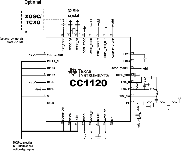
Very few external components are required for the operation of the CC1120 device. Figure 6-1 shows a typical application circuit. The board layout will greatly influence the RF performance of the CC1120 device. Figure 6-1 does not show decoupling capacitors for power pins.
 Figure 6-1 Typical Application Circuit
6.1.2 TI Reference Designs
The following reference designs are available for the CC1120 device:
-
CC1120EM-868-915-RDCC1120EM 868- to 915-MHz Reference Design
This RF Layout Reference Design demonstrates good decoupling and layout techniques for a low power RF device operating in the 868-MHz and 915-MHz frequency bands.
CC1120EM 868/915 MHz Reference Design (SWRC222)
CC112x IPC 868- and 915-MHz 2-layer Reference Design (SWRR106)
CC112x IPC 868- and 915-MHz 4-layer Reference Design (SWRR107)
-
CC1120EM-169-RDCC1120EM 169-MHz Reference Design
This RF Layout Reference Design demonstrates good decoupling and layout techniques for a low power RF device operating in the 169-MHz frequency band. (SWRC220)
-
CC1120EM-420-470-RDCC1120EM 420- to 470-MHz Reference Design
This RF Layout Reference Design demonstrates good decoupling and layout techniques for a low power RF device operating in the 420-470 MHz frequency band. (SWRC221)