SWRS045F January 2006 – November 2018 CC1021
PRODUCTION DATA.
- 1Device Overview
- 2Revision History
- 3Terminal Configuration and Functions
-
4Specifications
- 4.1 Absolute Maximum Ratings
- 4.2 ESD Ratings
- 4.3 Recommended Operating Conditions
- 4.4 RF Transmit
- 4.5 RF Receive
- 4.6 RSSI / Carrier Sense
- 4.7 Intermediate Frequency (IF)
- 4.8 Crystal Oscillator
- 4.9 Frequency Synthesizer
- 4.10 Digital Inputs / Outputs
- 4.11 Current Consumption
- 4.12 Thermal Resistance Characteristics for VQFNP Package
-
5Detailed Description
- 5.1 Overview
- 5.2 Functional Block Diagram
- 5.3 Configuration Overview
- 5.4 Microcontroller Interface
- 5.5 4-wire Serial Configuration Interface
- 5.6 Signal Interface
- 5.7 Data Rate Programming
- 5.8 Frequency Programming
- 5.9
Receiver
- 5.9.1 IF Frequency
- 5.9.2 Receiver Channel Filter Bandwidth
- 5.9.3 Demodulator, Bit Synchronizer and Data Decision
- 5.9.4 Receiver Sensitivity versus Data Rate and Frequency Separation
- 5.9.5 RSSI
- 5.9.6 Image Rejection Calibration
- 5.9.7 Blocking and Selectivity
- 5.9.8 Linear IF Chain and AGC Settings
- 5.9.9 AGC Settling
- 5.9.10 Preamble Length and Sync Word
- 5.9.11 Carrier Sense
- 5.9.12 Automatic Power-Up Sequencing
- 5.9.13 Automatic Frequency Control
- 5.9.14 Digital FM
- 5.10 Transmitter
- 5.11 Input and Output Matching and Filtering
- 5.12 Frequency Synthesizer
- 5.13 VCO and LNA Current Control
- 5.14 Power Management
- 5.15 On-Off Keying (OOK)
- 5.16 Crystal Oscillator
- 5.17 Built-in Test Pattern Generator
- 5.18 Interrupt on Pin DCLK
- 5.19 PA_EN and LNA_EN Digital Output Pins
- 5.20 System Considerations and Guidelines
- 5.21 Antenna Considerations
- 5.22 Configuration Registers
- 6Applications, Implementation, and Layout
- 7Device and Documentation Support
- 8Mechanical Packaging and Orderable Information
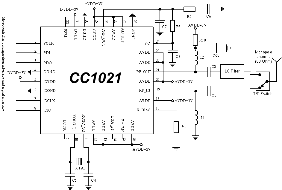
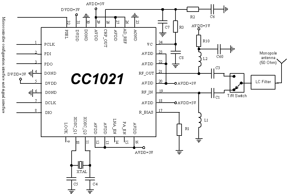
6.1.1 Typical Application
 Figure 6-1 Typical Application and Test Circuit (Power Supply Decoupling Not Shown)
  Figure 6-2 Alternative Application Circuit (Power Supply Decoupling Not Shown)
 Table 6-1 Overview of External Components (Excluding Supply Decoupling Capacitors)
| REF | DESCRIPTION |
|---|---|
| C1 | LNA input match and DC block, see Section 5.11 |
| C3 | PA output match and DC block, see Section 5.11 |
| C4 | Crystal load capacitor, see Section 5.16 |
| C5 | Crystal load capacitor, see Section 5.16 |
| C6 | PLL loop filter capacitor |
| C7 | PLL loop filter capacitor (may be omitted for highest loop bandwidth) |
| C8 | PLL loop filter capacitor (may be omitted for highest loop bandwidth) |
| C60 | Decoupling capacitor |
| L1 | LNA match and DC bias (ground), see Section 5.11 |
| L2 | PA match and DC bias (supply voltage), see Section 5.11 |
| R1 | Precision resistor for current reference generator |
| R2 | PLL loop filter resistor |
| R3 | PLL loop filter resistor |
| R10 | PA output match, see Section 5.11 |
| XTAL | Crystal, see Section 5.16 |
Table 6-2 Bill of Materials for the Application Circuit in Figure 6-1(1)(2)
| ITEM | 433 MHz | 868 MHz | 915 MHz |
|---|---|---|---|
| C1(3) | 10 pF, 5%, NP0, 0402 | 47 pF, 5%, NP0, 0402 | 47 pF, 5%, NP0, 0402 |
| C3(3) | 5.6 pF, 5%, NP0, 0402 | 10 pF, 5%, NP0, 0402 | 10 pF, 5%, NP0, 0402 |
| C4 | 22 pF, 5%, NP0, 0402 | 22 pF, 5%, NP0, 0402 | 22 pF, 5%, NP0, 0402 |
| C5 | 12 pF, 5%, NP0, 0402 | 12 pF, 5%, NP0, 0402 | 12 pF, 5%, NP0, 0402 |
| C6 | 3.9 nF, 10%, X7R, 0603 | 3.9 nF, 10%, X7R, 0603 | 3.9 nF, 10%, X7R, 0603 |
| C7 | 120 pF, 10%, X7R, 0402 | 120 pF, 10%, X7R, 0402 | 120 pF, 10%, X7R, 0402 |
| C8 | 33 pF, 10%, X7R, 0402 | 33 pF, 10%, X7R, 0402 | 33 pF, 10%, X7R, 0402 |
| C60 | 220 pF, 5%, NP0, 0402 | 220 pF, 5%, NP0, 0402 | 220 pF, 5%, NP0, 0402 |
| L1(3) | 33 nH, 5%, 0402 | 82 nH, 5%, 0402 | 82 nH, 5%, 0402 |
| L2(3) | 22 nH, 5%, 0402 | 3.6 nH, 5%, 0402 | 3.6 nH, 5%, 0402 |
| R1 | 82 kΩ, 1%, 0402 | 82 kΩ, 1%, 0402 | 82 kΩ, 1%, 0402 |
| R2 | 12 kΩ, 5%, 0402 | 12 kΩ, 5%, 0402 | 12 kΩ, 5%, 0402 |
| R3 | 39 kΩ, 5%, 0402 | 39 kΩ, 5%, 0402 | 39 kΩ, 5%, 0402 |
| R10 | 82 Ω, 5%, 0402 | 82 Ω, 5%, 0402 | 82 Ω, 5%, 0402 |
| XTAL | 14.7456 MHz crystal, 16 pF load | 14.7456 MHz crystal, 16 pF load | 14.7456 MHz crystal, 16 pF load |
In the CC1020EMX reference design, which is also applicable for the CC1021 device, LQG15HS series inductors from Murata have been used. The switch is SW-456 from M/A-COM.
The LC filter in Figure 6-1 is inserted in the TX path only. The filter will reduce the emission of harmonics and the spurious emissions in the TX path. An alternative is to insert the LC filter between the antenna and the T/R switch as shown in Figure 6-2.
The filter will reduce the emission of harmonics and the spurious emissions in the TX path as well as increase the receiver selectivity. The sensitivity will be slightly reduced due to the insertion loss of the LC filter.