ZHCSG63C December 2013 – July 2018
PRODUCTION DATA.
- 1 特性
- 2 应用
- 3 说明
- 4 修订历史记录
- 5 Device Comparison Table
- 6 Pin Configuration and Functions
- 7 Specifications
-
8 Detailed Description
- 8.1 Overview
- 8.2 Functional Block Diagram
- 8.3
Feature Description
- 8.3.1 Details of a Qi Wireless Power System and bq51003 Power Transfer Flow Diagrams
- 8.3.2 Dynamic Rectifier Control
- 8.3.3 Dynamic Efficiency Scaling
- 8.3.4 RILIM Calculations
- 8.3.5 Input Overvoltage
- 8.3.6 Adapter Enable Functionality and EN1/EN2 Control
- 8.3.7 End Power Transfer Packet (WPC Header 0x02)
- 8.3.8 Status Outputs
- 8.3.9 WPC Communication Scheme
- 8.3.10 Communication Modulator
- 8.3.11 Adaptive Communication Limit
- 8.3.12 Synchronous Rectification
- 8.3.13 Temperature Sense Resistor Network (TS)
- 8.3.14 3-State Driver Recommendations for the TS-CTRL Pin
- 8.3.15 Thermal Protection
- 8.3.16 WPC v1.2 Compliance – Foreign Object Detection
- 8.4 Device Functional Modes
- 9 Application and Implementation
- 10Power Supply Recommendations
- 11Layout
- 12器件和文档支持
- 13机械、封装和可订购信息
9.2.1.3 Application Curves
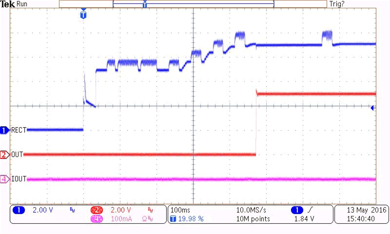
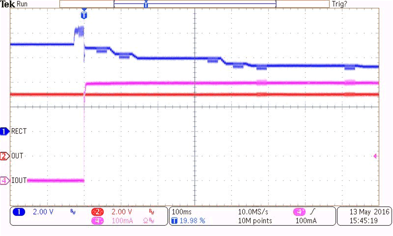
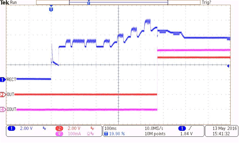
The following figures show the bq51003EVM-764 under 3 conditions. The RECT pin signal shows the bq51003 rectifier response due to the changing conditions. The OUT pin signal shows the impact to the OUT pin during the changed conditions. IOUT shows the current being sourced by the OUT pin.
Figure 35 shows the bq51003EVM-764 being placed on a transmitter with no load at the OUT pin. This shows the RECT pin receiving the Ping from the transmitter and responding with identification and other packets to establish power transfer. Once the RECT pin has reached its required voltage, the OUT pin is enabled and produces 5 V. The communication packet after 5 V is produced indicates the steady state condition being sent to the transmitter.
Figure 36 shows the same conditions, but the OUT pin has a resistive load which produces 400 mA at 5 V. The OUT pin current, IOUT, increases with the OUT pin voltage. The communication packets that occur after IOUT increases are sent to adjust the RECT voltge to the appropriate level.
Figure 37 shows the bq51003 under a no load condition until a 400-mA resistive load is added. Communication packets are sent until the RECT has come to the appropriate steady state value.
 Figure 35. bq51003 Added to TX With No Load
  Figure 37. bq51003 – No Load to 400-mA Resistive Load
  Figure 36. bq51003 Added to TX With 400-mA Resistive Load