ZHCSG63C December 2013 – July 2018
PRODUCTION DATA.
- 1 特性
- 2 应用
- 3 说明
- 4 修订历史记录
- 5 Device Comparison Table
- 6 Pin Configuration and Functions
- 7 Specifications
-
8 Detailed Description
- 8.1 Overview
- 8.2 Functional Block Diagram
- 8.3
Feature Description
- 8.3.1 Details of a Qi Wireless Power System and bq51003 Power Transfer Flow Diagrams
- 8.3.2 Dynamic Rectifier Control
- 8.3.3 Dynamic Efficiency Scaling
- 8.3.4 RILIM Calculations
- 8.3.5 Input Overvoltage
- 8.3.6 Adapter Enable Functionality and EN1/EN2 Control
- 8.3.7 End Power Transfer Packet (WPC Header 0x02)
- 8.3.8 Status Outputs
- 8.3.9 WPC Communication Scheme
- 8.3.10 Communication Modulator
- 8.3.11 Adaptive Communication Limit
- 8.3.12 Synchronous Rectification
- 8.3.13 Temperature Sense Resistor Network (TS)
- 8.3.14 3-State Driver Recommendations for the TS-CTRL Pin
- 8.3.15 Thermal Protection
- 8.3.16 WPC v1.2 Compliance – Foreign Object Detection
- 8.4 Device Functional Modes
- 9 Application and Implementation
- 10Power Supply Recommendations
- 11Layout
- 12器件和文档支持
- 13机械、封装和可订购信息
8.3.10 Communication Modulator
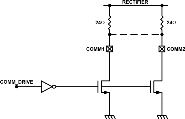
The bq51003 provides two identical, integrated communication FETs which are connected to the pins COMM1 and COMM2. These FETs are used for modulating the secondary load current which allows bq51003 to communicate error control and configuration information to the transmitter. Figure 26 shows how the COMM pins can be used for resistive load modulation. Each COMM pin can handle at most a 24-Ω communication resistor. Therefore, if a COMM resistor between 12 Ω and 24 Ω is required COMM1 and COMM2 pins must be connected in parallel. The bq51003 does not support a COMM resistor less than 12 Ω.
 Figure 26. Resistive Load Modulation
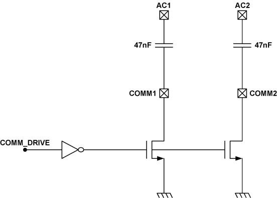
 In addition to resistive load modulation, the bq51003 is also capable of capacitive load modulation as shown in Figure 27. In this case, a capacitor is connected from COMM1 to AC1 and from COMM2 to AC2. When the COMM switches are closed there is effectively a 22-nF capacitor connected between AC1 and AC2. Connecting a capacitor in between AC1 and AC2 modulates the impedance seen by the coil, which will be reflected in the primary as a change in current.
 Figure 27. Capacitive Load Modulation