ZHCSJ56C February   2018  – September 2019 BQ25882

PRODUCTION DATA.  

  1. 特性
  2. 应用
  3. 说明
    1.     简化原理图
      1.      Device Images
  4. 修订历史记录
  5. Device Comparison Table
  6. Pin Configuration and Functions
    1.     Pin Functions
  7. Specifications
    1. 7.1 Absolute Maximum Ratings
    2. 7.2 ESD Ratings
    3. 7.3 Recommended Operating Conditions
    4. 7.4 Thermal Information
    5. 7.5 Electrical Characteristics
    6. 7.6 Timing Requirements
    7. 7.7 Typical Characteristics
  8. Detailed Description
    1. 8.1 Overview
    2. 8.2 Functional Block Diagram
    3. 8.3 Feature Description
      1. 8.3.1  Device Power-On-Reset
      2. 8.3.2  Device Power Up from Battery without Input Source
      3. 8.3.3  Device Power Up from Input Source
        1. 8.3.3.1 Poor Source Qualification
        2. 8.3.3.2 Input Source Type Detection
          1. 8.3.3.2.1 D+/D– Detection Sets Input Current Limit
          2. 8.3.3.2.2 Force Input Current Limit Detection
        3. 8.3.3.3 Power up REGN Regulator (LDO)
        4. 8.3.3.4 Converter Power Up
      4. 8.3.4  Input Current Optimizer (ICO)
      5. 8.3.5  Buck Mode Operation from Battery (OTG)
      6. 8.3.6  Power Path Management
        1. 8.3.6.1 Narrow VDC Architecture
        2. 8.3.6.2 Dynamic Power Management
        3. 8.3.6.3 Supplement Mode
      7. 8.3.7  Battery Charging Management
        1. 8.3.7.1 Autonomous Charging Cycle
        2. 8.3.7.2 Battery Charging Profile
        3. 8.3.7.3 Charging Termination
        4. 8.3.7.4 Thermistor Qualification
          1. 8.3.7.4.1 JEITA Guideline Compliance in Charge Mode
          2. 8.3.7.4.2 Cold/Hot Temperature Window in OTG Buck Mode
        5. 8.3.7.5 Charging Safety Timer
      8. 8.3.8  Integrated 16-Bit ADC for Monitoring
      9. 8.3.9  Status Outputs (PG, and INT)
        1. 8.3.9.1 Power Good Indicator (PG)
        2. 8.3.9.2 Interrupt to Host (INT)
      10. 8.3.10 Input Current Limit on ILIM Pin
      11. 8.3.11 Voltage and Current Monitoring
        1. 8.3.11.1 Voltage and Current Monitoring in Boost Mode
          1. 8.3.11.1.1 Input Over-voltage Protection
          2. 8.3.11.1.2 Input Under-Voltage Protection
          3. 8.3.11.1.3 System Over-Voltage Protection
          4. 8.3.11.1.4 System Over-Current Protection
        2. 8.3.11.2 Voltage and Current Monitoring in OTG Buck Mode
          1. 8.3.11.2.1 VBUS Over-Voltage Protection
          2. 8.3.11.2.2 VBUS Over-Current Protection
      12. 8.3.12 Thermal Regulation and Thermal Shutdown
        1. 8.3.12.1 Thermal Protection in Boost Mode
        2. 8.3.12.2 Thermal Protection in OTG Buck Mode
      13. 8.3.13 Battery Protection
        1. 8.3.13.1 Battery Overvoltage Protection (BATOVP)
        2. 8.3.13.2 Battery Over-Discharge Protection
      14. 8.3.14 Serial Interface
        1. 8.3.14.1 Data Validity
        2. 8.3.14.2 START and STOP Conditions
        3. 8.3.14.3 Byte Format
        4. 8.3.14.4 Acknowledge (ACK) and Not Acknowledge (NACK)
        5. 8.3.14.5 Slave Address and Data Direction Bit
        6. 8.3.14.6 Single Write and Read
        7. 8.3.14.7 Multi-Write and Multi-Read
    4. 8.4 Device Functional Modes
      1. 8.4.1 Host Mode and Default Mode
    5. 8.5 Register Maps
      1. 8.5.1  Battery Voltage Regulation Limit Register (Address = 00h) [reset = A0h]
        1. Table 9. REG00 Register Field Descriptions
      2. 8.5.2  Charger Current Limit Register (Address = 01h) [reset = 54h]
        1. Table 10. REG01 Register Field Descriptions
      3. 8.5.3  Input Voltage Limit Register (Address = 02h) [reset = 85h]
        1. Table 11. REG02 Register Field Descriptions
      4. 8.5.4  Input Current Limit Register (Address = 03h) [reset = 39h]
        1. Table 12. REG03 Register Field Descriptions
      5. 8.5.5  Precharge and Termination Current Limit Register (Address = 04h) [reset = 22h]
        1. Table 13. REG04 Register Field Descriptions
      6. 8.5.6  Charger Control 1 Register (Address = 05h) [reset = 9Dh]
        1. Table 14. REG05 Register Field Descriptions
      7. 8.5.7  Charger Control 2 Register (Address = 06h) [reset = 7Dh]
        1. Table 15. REG06 Register Field Descriptions
      8. 8.5.8  Charger Control 3 Register (Address = 07h) [reset = 0Ah]
        1. Table 16. REG07 Register Field Descriptions
      9. 8.5.9  Charger Control 4 Register (Address = 08h) [reset = 0Dh]
        1. Table 17. REG08 Register Field Descriptions
      10. 8.5.10 OTG Control Register (Address = 09h) [reset = F6h]
        1. Table 18. REG09 Register Field Descriptions
      11. 8.5.11 ICO Current Limit Register (Address = 0Ah) [reset = XXh]
        1. Table 19. REG0A Register Field Descriptions
      12. 8.5.12 Charger Status 1 Register (Address = 0Bh) [reset = XXh]
        1. Table 20. REG0B Register Field Descriptions
      13. 8.5.13 Charger Status 2 Register (Address = 0Ch) [reset = XXh]
        1. Table 21. REG0C Register Field Descriptions
      14. 8.5.14 NTC Status Register (Address = 0Dh) [reset = 0Xh]
        1. Table 22. REG0D Register Field Descriptions
      15. 8.5.15 FAULT Status Register (Address = 0Eh) [reset = XXh]
        1. Table 23. REG0E Register Field Descriptions
      16. 8.5.16 Charger Flag 1 Register (Address = 0Fh) [reset = 00h]
        1. Table 24. REG0F Register Field Descriptions
      17. 8.5.17 Charger Flag 2 Register (Address = 10h) [reset = 00h]
        1. Table 25. REG10 Register Field Descriptions
      18. 8.5.18 FAULT Flag Register (Address = 11h) [reset = 00h]
        1. Table 26. REG11 Register Field Descriptions
      19. 8.5.19 Charger Mask 1 Register (Address = 12h) [reset = 00h]
        1. Table 27. REG12 Register Field Descriptions
      20. 8.5.20 Charger Mask 2 Register (Address = 13h) [reset = 00h]
        1. Table 28. REG13 Register Field Descriptions
      21. 8.5.21 FAULT Mask Register (Address = 14h) [reset = 00h]
        1. Table 29. REG14 Register Field Descriptions
      22. 8.5.22 ADC Control Register (Address = 15h) [reset = 30h]
        1. Table 30. REG15 Register Field Descriptions
      23. 8.5.23 ADC Function Disable Register (Address = 16h) [reset = 00h]
        1. Table 31. REG16 Register Field Descriptions
      24. 8.5.24 IBUS ADC 1 Register (Address = 17h) [reset = 00h]
        1. Table 32. REG17 Register Field Descriptions
      25. 8.5.25 IBUS ADC 0 Register (Address = 18h) [reset = 00h]
        1. Table 33. REG18 Register Field Descriptions
      26. 8.5.26 ICHG ADC 1 Register (Address = 19h) [reset = 00h]
        1. Table 34. REG19 Register Field Descriptions
      27. 8.5.27 ICHG ADC 0 Register (Address = 1Ah) [reset = 00h]
        1. Table 35. REG1A Register Field Descriptions
      28. 8.5.28 VBUS ADC 1 Register (Address = 1Bh) [reset = 00h]
        1. Table 36. REG1B Register Field Descriptions
      29. 8.5.29 VBUS ADC 0 Register (Address = 1Ch) [reset = 00h]
        1. Table 37. REG1C Register Field Descriptions
      30. 8.5.30 VBAT ADC 1 Register (Address = 1Dh) [reset = 00h]
        1. Table 38. REG1D Register Field Descriptions
      31. 8.5.31 VBAT ADC 0 Register (Address = 1Eh) [reset = 00h]
        1. Table 39. REG1E Register Field Descriptions
      32. 8.5.32 VSYS ADC 1 Register (Address = 1Fh) [reset = 00h]
        1. Table 40. REG1F Register Field Descriptions
      33. 8.5.33 VSYS ADC 0 Register (Address = 20h) [reset = 00h]
        1. Table 41. REG20 Register Field Descriptions
      34. 8.5.34 TS ADC 1 Register (Address = 21h) [reset = 00h]
        1. Table 42. REG21 Register Field Descriptions
      35. 8.5.35 TS ADC 0 Register (Address = 22h) [reset = 00h]
        1. Table 43. REG22 Register Field Descriptions
      36. 8.5.36 TDIE ADC 1 Register (Address = 23h) [reset = 00h]
        1. Table 44. REG23 Register Field Descriptions
      37. 8.5.37 TDIE ADC 0 Register (Address = 24h) [reset = 00h]
        1. Table 45. REG24 Register Field Descriptions
      38. 8.5.38 Part Information Register (Address = 25h) [reset = 11h]
        1. Table 46. REG25 Register Field Descriptions
  9. Application and Implementation
    1. 9.1 Application Information
    2. 9.2 Typical Application
      1. 9.2.1 Design Requirements
      2. 9.2.2 Detailed Design Procedure
        1. 9.2.2.1 Inductor Selection
        2. 9.2.2.2 Input (VBUS / PMID) Capacitor
        3. 9.2.2.3 Output (VSYS) Capacitor
      3. 9.2.3 Application Curves
  10. 10Power Supply Recommendations
  11. 11Layout
    1. 11.1 Layout Guidelines
    2. 11.2 Layout Example
  12. 12器件和文档支持
    1. 12.1 器件支持
      1. 12.1.1 第三方产品免责声明
        1. 12.1.1.1 第三方产品免责声明
    2. 12.2 文档支持
      1. 12.2.1 相关文档
    3. 12.3 接收文档更新通知
    4. 12.4 社区资源
    5. 12.5 商标
    6. 12.6 静电放电警告
    7. 12.7 Glossary
  13. 13机械、封装和可订购信息

封装选项

机械数据 (封装 | 引脚)
散热焊盘机械数据 (封装 | 引脚)
订购信息

Input Current Limit on ILIM Pin

For safe operation, the device has an additional hardware pin on ILIM to limit maximum input current. The maximum input current is set by a resistor from ILIM pin to ground as:

Equation 3. BQ25882 IINMAX_eqn3.gif

The actual input current limit is the lower value between ILIM pin setting and register setting (IINDPM). For example, if the register setting is 3.3 A (0x1C), and ILIM has a 820-Ω resistor to ground, the input current limit is 1.43 A (KILIM = 1170 max). ILIM pin can be used to set the input current limit rather than the register settings when EN_ILIM bit is set. The device regulates ILIM pin at 0.8 V. If ILIM voltage exceeds 0.8 V, the device enters input current regulation (refer to Dynamic Power Management section). Entering IINDPM through ILIM pin sets the IINDPM_STAT and FLAG bits, and produces an interrupt to host. The interrupt can be masked via the IINDPM_MASK bit.

The ILIM pin can also be used to monitor input current when EN_ILIM is set and the device is not in ILIM regulation. The voltage on ILIM pin is proportional to the input current. ILIM can be used to monitor input current with the following relationship:
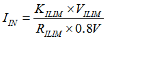
Equation 4. BQ25882 IIN_eqn4.gif

For example, if ILIM pin is set with 820-Ω resistor, and the ILIM voltage 0.5 V, the actual input current is 0.762 A to 0.892 A (based on KILIM specified). If ILIM pin is open, the input current is limited to zero since ILIM voltage floats above 0.8 V. If ILIM pin is shorted, the input current limit is set by the register.

The ILIM pin function can be disabled by setting the EN_ILIM bit to 0. When the pin is disabled, both input current limit function and monitoring function are not available.