SPRS550F October 2009 – July 2014 AM3505 , AM3517
PRODUCTION DATA.
- 1Device Summary
- 2Revision History
- 3Device Comparison
- 4Terminal Configuration and Functions
- 5Specifications
-
6Timing Requirements and Switching Characteristics
- 6.1 Timing Test Conditions
- 6.2 Interface Clock Specifications
- 6.3 Timing Parameters
- 6.4
External Memory Interfaces
- 6.4.1 General-Purpose Memory Controller (GPMC)
- 6.4.2
SDRAM Controller (SDRC)
- 6.4.2.1 LPDDR Interface
- 6.4.2.2
DDR2 Interface
- 6.4.2.2.1 DDR2 Interface Schematic
- 6.4.2.2.2 Compatible JEDEC DDR2 Devices
- 6.4.2.2.3 PCB Stackup
- 6.4.2.2.4 Placement
- 6.4.2.2.5 DDR2 Keep Out Region
- 6.4.2.2.6 Bulk Bypass Capacitors
- 6.4.2.2.7 High-Speed Bypass Capacitors
- 6.4.2.2.8 Net Classes
- 6.4.2.2.9 DDR2 Signal Termination
- 6.4.2.2.10 VREF Routing
- 6.4.2.2.11 DDR2 CLK and ADDR_CTRL Routing
- 6.4.2.2.12 On Die Termination (ODT)
- 6.5 Video Interfaces
- 6.6
Serial Communications Interfaces
- 6.6.1 Multichannel Buffered Serial Port (McBSP) Timing
- 6.6.2 Multichannel Serial Port Interface (McSPI) Timing
- 6.6.3 Multiport Full-Speed Universal Serial Bus (USB) Interface
- 6.6.4 Multiport High-Speed Universal Serial Bus (USB) Timing
- 6.6.5 USB0 OTG (USB2.0 OTG)
- 6.6.6 High-End Controller Area Network Controller (HECC) Timing
- 6.6.7 Ethernet Media Access Controller (EMAC)
- 6.6.8 Management Data Input/Output (MDIO)
- 6.6.9 Universal Asynchronous Receiver/Transmitter (UART)
- 6.6.10 HDQ / 1-Wire Interfaces
- 6.6.11 I2C Interface
- 6.7 Removable Media Interfaces
- 6.8 Test Interfaces
- 7Device and Documentation Support
- 8Mechanical Packaging and Orderable Information
封装选项
请参考 PDF 数据表获取器件具体的封装图。
机械数据 (封装 | 引脚)
- ZER|484
- ZCN|491
散热焊盘机械数据 (封装 | 引脚)
订购信息
6 Timing Requirements and Switching Characteristics
Note: The timing data shown is preliminary data and is subject to change in future revisions.
6.1 Timing Test Conditions
All timing requirements and switching characteristics are valid over the recommended operating conditions of Table 5-3, unless otherwise specified.
6.2 Interface Clock Specifications
6.2.1 Interface Clock Terminology
The Interface clock is used at the system level to sequence the data and/or control transfers accordingly with the interface protocol.
6.2.2 Interface Clock Frequency
The two interface clock characteristics are:
- The maximum clock frequency
- The maximum operating frequency
The interface clock frequency documented in this document is the maximum clock frequency, which corresponds to the maximum frequency programmable on this output clock. This frequency defines the maximum limit supported by the AM3517/05 IC and does not take into account any system consideration (PCB, peripherals).
The system designer will have to consider these system considerations and AM3517/05 IC timings characteristics as well, to define properly the maximum operating frequency, which corresponds to the maximum frequency supported to transfer the data on this interface.
6.2.3 Clock Jitter Specifications
Jitter is a phase noise, which may alter different characteristics of a clock signal. The jitter specified in this document is the time difference between the typical cycle period and the actual cycle period affected by noise sources on the clock. The cycle (or period) jitter terminology identifies this type of jitter.
 Figure 6-1 Cycle (or Period) Jitter
6.2.4 Clock Duty Cycle Error
The maximum duty cycle error is the difference between the absolute value of the maximum high-level pulse duration or the maximum low-level pulse duration and the typical pulse duration value:
- Maximum pulse duration = typical pulse duration + maximum duty cycle error
- Minimum pulse duration = typical pulse duration - maximum duty cycle error
6.3 Timing Parameters
The timing parameter symbols used in the timing requirement and switching characteristic tables are created in accordance with JEDEC Standard 100. To shorten the symbols, some pin names and other related terminologies have been abbreviated as follows:
Table 6-1 Timing Parameters
| LOWERCASE SUBSCRIPTS | |
|---|---|
| Symbols | Parameter |
| c | Cycle time (period) |
| d | Delay time |
| dis | Disable time |
| en | Enable time |
| h | Hold time |
| su | Setup time |
| START | Start bit |
| t | Transition time |
| v | Valid time |
| w | Pulse duration (width) |
| X | Unknown, changing, or dont care level |
| H | High |
| L | Low |
| V | Valid |
| IV | Invalid |
| AE | Active Edge |
| FE | First Edge |
| LE | Last Edge |
| Z | High impedance |
6.4 External Memory Interfaces
The AM3517/05 processor includes the following external memory interfaces:
- General-purpose memory controller (GPMC)
- SDRAM controller (SDRC)
6.4.1 General-Purpose Memory Controller (GPMC)
The GPMC is the AM3517/05 unified memory controller used to interface external memory devices such as:
- Asynchronous SRAM-like memories and ASIC devices
- Asynchronous page mode and synchronous burst NOR flash
- NAND flash
6.4.1.1 GPMC/NOR Flash Interface Synchronous Timing
Table 6-2 through Table 6-4 assume testing over the recommended operating conditions and electrical characteristic conditions.
Table 6-2 GPMC/NOR Flash Synchronous Mode Timing Conditions
| TIMING CONDITION PARAMETER | 1.8V, 3.3V | UNIT | ||
|---|---|---|---|---|
| MIN | MAX | |||
| Input Conditions | ||||
| tR | Input signal rise time | 0.3 | 1.8 | ns |
| tF | Input signal fall time | 0.3 | 1.8 | ns |
| Output Conditions | ||||
| CLOAD | Output load capacitance | 30 | pF | |
Table 6-3 GPMC/NOR Flash Interface Timing Requirements Synchronous Mode
| NO. | PARAMETER | 1.8V, 3.3V | UNIT | ||
|---|---|---|---|---|---|
| MIN | MAX | ||||
| F12 | tsu(DV-CLKH) | Setup time, read gpmc_d[15:0] valid before gpmc_clk high | 2.021 | ns | |
| F13 | th(CLKH-DV) | Hold time, gpmc_d[15:0] valid after gpmc_clk high | 3.403 | ns | |
| F21 | tsu(WAITV-CLKH) | Setup time, gpmc_waitx(1) valid before gpmc_clk high | 3.782 | ns | |
| F22 | th(CLKH-WAITV) | Hold Time, gpmc_waitx(1) valid after gpmc_clk high | 3.343 | ns | |
Table 6-4 GPMC/NOR Flash Interface Switching Characteristics Synchronous Mode
| NO. | PARAMETER | 1.8V, 3.3V | UNIT | |||
|---|---|---|---|---|---|---|
| MIN | MAX | |||||
| F0 | tc(CLK) | Cycle time(14), output clock gpmc_clk period | 10 | ns | ||
| F1 | tw(CLKH) | Typical pulse duration, output clock gpmc_clk high | 0.5 P(12) | 0.5 P(12) | ns | |
| F1 | tw(CLKL) | Typical pulse duration, output clock gpmc_clk low | 0.5 P(12) | 0.5 P(12) | ns | |
| tdc(CLK) | Duty cycle error, output clk gpmc_clk | -500 | 500 | ps | ||
| tj(CLK) | Jitter standard deviation(15), output clock gpmc_clk | 33.30 | ps | |||
| tR(CLK) | Rise time, output clock gpmc_clk | 1.6 | ns | |||
| tF(CLK) | Fall time, output clock gpmc_clk | 1.6 | ns | |||
| tR(DO) | Rise time, output data | 2 | ns | |||
| tF(DO) | Fall time, output data | 2 | ns | |||
| F2 | td(CLKH-nCSV) | Delay time, gpmc_clk rising edge to gpmc_ncsx(11) transition | F(6) - 1.9 | F(6) + 3.3 | ns | |
| F3 | td(CLKH-nCSIV) | Delay time, gpmc_clk rising edge to gpmc_ncsx(11) invalid | E(5) - 1.9 | E(5) + 3.3 | ns | |
| F4 | td(ADDV-CLK) | Delay time, address bus valid to gpmc_clk first edge | B(2) - 4.1 | B(2) + 2.1 | ns | |
| F5 | td(CLKH-ADDIV) | Delay time, gpmc_clk rising edge to gpmc_a[16:1] invalid | -2.103 | ns | ||
| F6 | td(nBEV-CLK) | Delay time, gpmc_nbe0_cle, gpmc_nbe1 valid to gpmc_clk first edge | B(2) - 1.37 | B(2) + 2.1 | ns | |
| F7 | td(CLKH-nBEIV) | Delay time, gpmc_clk rising edge to gpmc_nbe0_cle, gpmc_nbe1 invalid | D(4) - 2.1 | D(4) + 1.1 | ns | |
| F8 | td(CLKH-nADV) | Delay time, gpmc_clk rising edge to gpmc_nadv_ale transition | G(7) - 1.9 | G(7) + 4.1 | ns | |
| F9 | td(CLKH-nADVIV) | Delay time, gpmc_clk rising edge to gpmc_nadv_ale invalid | D(4) - 1.9 | D(4) + 4.1 | ns | |
| F10 | td(CLKH-nOE) | Delay time, gpmc_clk rising edge to gpmc_noe transition | H(8) - 2.1 | H(8) + 2.1 | ns | |
| F11 | td(CLKH-nOEIV) | Delay time, gpcm rising edge to gpmc_noe invalid | E(5) - 2.1 | E(5) + 2.1 | ns | |
| F14 | td(CLKH-nWE) | Delay time, gpmc_clk rising edge to gpmc_nwe transition | I(9) - 1.9 | I(9) + 4.1 | ns | |
| F15 | td(CLKH-Data) | Delay time, gpmc_clk rising edge to data bus transition | J(10) - 2.1 | J(10) + 1.1 | ns | |
| F17 | td(CLKH-nBE) | Delay time, gpmc_clk rising edge to gpmc_nbex_cle transition | J(10) - 2.1 | J(10) + 1.1 | ns | |
| F18 | tW(nCSV) | Pulse duration, gpmc_ncsx(11) low | Read | A(1) | ns | |
| Write | A(1) | ns | ||||
| F19 | tW(nBEV) | Pulse duration, gpmc_nbe0_cle, gpmc_nbe1 low | Read | C(3) | ns | |
| Write | C(3) | ns | ||||
| F20 | tW(nADVV) | Pulse duration, gpmc_nadv_ale low | Read | K(13) | ns | |
| Write | K(13) | ns | ||||
| F23 | td(CLKH-IODIR) | Delay time, gpmc_clk rising edge to gpmc_io_dir high (IN direction) | H(8) - 2.1 | H(8) + 4.1 | ns | |
| F24 | td(CLKH-IODIRIV) | Delay time, gpmc_clk rising edge to gpmc_io_dir low (OUT direction) | M(16) - 2.1 | M(16) + 4.1 | ns | |
For burst read: A = (CSRdOffTime - CSOnTime + (n 1) * PageBurstAccessTime) * (TimeParaGranularity + 1) * GPMC_FCLK period
For burst write: A = (CSWrOffTime - CSOnTime + (n 1) * PageBurstAccessTime) * (TimeParaGranularity + 1) * GPMC_FCLK period with n being the page burst access number.
For burst read: C = (RdCycleTime + (n 1) * PageBurstAccessTime) * (TimeParaGranularity + 1) * GPMC_FCLK
For burst write: C = (WrCycleTime + (n 1) * PageBurstAccessTime) * (TimeParaGranularity + 1) * GPMC_FCLK with n being the page burst access number.
For burst read: D = (RdCycleTime - AccessTime) * (TimeParaGranularity + 1) * GPMC_FCLK
For burst write: D = (WrCycleTime - AccessTime) * (TimeParaGranularity + 1) * GPMC_FCLK
For burst read: E = (CSRdOffTime - AccessTime) * (TimeParaGranularity + 1) * GPMC_FCLK
For burst write: E = (CSWrOffTime - AccessTime) * (TimeParaGranularity + 1) * GPMC_FCLK
-
Case GpmcFCLKDivider = 0:
- F = 0.5 * CSExtraDelay * GPMC_FCLK
-
Case GpmcFCLKDivider = 1:
- F = 0.5 * CSExtraDelay * GPMC_FCLK if (ClkActivationTime and CSOnTime are odd) or (ClkActivationTime and CSOnTime are even)
- F = (1 + 0.5 * CSExtraDelay) * GPMC_FCLK otherwise
-
Case GpmcFCLKDivider = 2:
- F = 0.5 * CSExtraDelay * GPMC_FCLK if ((CSOnTime - ClkActivationTime) is a multiple of 3)
- F = (1 + 0.5 * CSExtraDelay) * GPMC_FCLK if ((CSOnTime - ClkActivationTime - 1) is a multiple of 3)
- F = (2 + 0.5 * CSExtraDelay) * GPMC_FCLK if ((CSOnTime - ClkActivationTime - 2) is a multiple of 3)
-
Case GpmcFCLKDivider = 0:
- G = 0.5 * ADVExtraDelay * GPMC_FCLK
-
Case GpmcFCLKDivider = 1:
- G = 0.5 * ADVExtraDelay * GPMC_FCLK if (ClkActivationTime and ADVOnTime are odd) or (ClkActivationTime and ADVOnTime are even)
- G = (1 + 0.5 * ADVExtraDelay) * GPMC_FCLK otherwise
-
Case GpmcFCLKDivider = 2:
- G = 0.5 * ADVExtraDelay * GPMC_FCLK if ((ADVOnTime - ClkActivationTime) is a multiple of 3)
- G = (1 + 0.5 * ADVExtraDelay) * GPMC_FCLK if ((ADVOnTime - ClkActivationTime - 1) is a multiple of 3)
- G = (2 + 0.5 * ADVExtraDelay) * GPMC_FCLK if ((ADVOnTime --ClkActivationTime - 2) is a multiple of 3)
For ADV rising edge (ADV deactivated) in Reading mode:
-
Case GpmcFCLKDivider = 0:
- G = 0.5 * ADVExtraDelay * GPMC_FCLK
-
Case GpmcFCLKDivider = 1:
- G = 0.5 * ADVExtraDelay * GPMC_FCLK if (ClkActivationTime and ADVRdOffTime are odd) or (ClkActivationTime and ADVRdOffTime are even)
- G = (1 + 0.5 * ADVExtraDelay) * GPMC_FCLK otherwise
- Case GpmcFCLKDivider = 2:
- G = 0.5 * ADVExtraDelay * GPMC_FCLK if ((ADVRdOffTime - ClkActivationTime) is a multiple of 3)
- G = (1 + 0.5 * ADVExtraDelay) * GPMC_FCLK if ((ADVRdOffTime --ClkActivationTime --1) is a multiple of 3)
- G = (2 + 0.5 * ADVExtraDelay) * GPMC_FCLK if ((ADVRdOffTime --ClkActivationTime - 2) is a multiple of 3)
For ADV rising edge (ADV deactivated) in Writing mode:
-
Case GpmcFCLKDivider = 0:
- G = 0.5 * ADVExtraDelay * GPMC_FCLK
-
Case GpmcFCLKDivider = 1:
- G = 0.5 * ADVExtraDelay * GPMC_FCLK if (ClkActivationTime and ADVWrOffTime are odd) or (ClkActivationTime and ADVWrOffTime are even)
- G = (1 + 0.5 * ADVExtraDelay) * GPMC_FCLK otherwise
-
Case GpmcFCLKDivider = 2:
- G = 0.5 * ADVExtraDelay * GPMC_FCLK if ((ADVWrOffTime - ClkActivationTime) is a multiple of 3)
- G = (1 + 0.5 * ADVExtraDelay) * GPMC_FCLK if ((ADVWrOffTime - ClkActivationTime - 1) is a multiple of 3)
- G = (2 + 0.5 * ADVExtraDelay) * GPMC_FCLK if ((ADVWrOffTime - ClkActivationTime - 2) is a multiple of 3)
-
Case GpmcFCLKDivider = 0:
- H = 0.5 * OEExtraDelay * GPMC_FCLK
-
Case GpmcFCLKDivider = 1:
- H = 0.5 * OEExtraDelay * GPMC_FCLK if (ClkActivationTime and OEOnTime are odd) or (ClkActivationTime and OEOnTime are even)
- H = (1 + 0.5 * OEExtraDelay) * GPMC_FCLK otherwise
-
Case GpmcFCLKDivider = 2:
- H = 0.5 * OEExtraDelay * GPMC_FCLK if ((OEOnTime - ClkActivationTime) is a multiple of 3)
- H = (1 + 0.5 * OEExtraDelay) * GPMC_FCLK if ((OEOnTime - ClkActivationTime - 1) is a multiple of 3)
- H = (2 + 0.5 * OEExtraDelay) * GPMC_FCLK if ((OEOnTime - ClkActivationTime - 2) is a multiple of 3)
For OE rising edge (OE deactivated):
-
GpmcFCLKDivider = 0:
- H = 0.5 * OEExtraDelay * GPMC_FCLK
-
Case GpmcFCLKDivider = 1:
- H = 0.5 * OEExtraDelay * GPMC_FC if (ClkActivationTime and OEOffTime are odd) or (ClkActivationTime and OEOffTime are even)
- H = (1 + 0.5 * OEExtraDelay) * GPMC_FCLK otherwise
-
Case GpmcFCLKDivider = 2:
- H = 0.5 * OEExtraDelay * GPMC_FCLK if ((OEOffTime - ClkActivationTime) is a multiple of 3)
- H = (1 + 0.5 * OEExtraDelay) * GPMC_FCLK if ((OEOffTime - ClkActivationTime - 1) is a multiple of 3)
- H = (2 + 0.5 * OEExtraDelay) * GPMC_FCLK if ((OEOffTime - ClkActivationTime - 2) is a multiple of 3)
-
Case GpmcFCLKDivider = 0:
- I = 0.5 * WEExtraDelay * GPMC_FCLK
-
Case GpmcFCLKDivider = 1:
- I = 0.5 * WEExtraDelay * GPMC_FCLK if (ClkActivationTime and WEOnTime are odd) or (ClkActivationTime and WEOnTime are even)
- I = (1 + 0.5 * WEExtraDelay) * GPMC_FCLK otherwise
-
Case GpmcFCLKDivider = 2:
- I = 0.5 * WEExtraDelay * GPMC_FCLK if ((WEOnTime - ClkActivationTime) is a multiple of 3)
- I = (1 + 0.5 * WEExtraDelay) * GPMC_FCLK if ((WEOnTime --ClkActivationTime - 1) is a multiple of 3)
- I = (2 + 0.5 * WEExtraDelay) * GPMC_FCLK if ((WEOnTime - ClkActivationTime - 2) is a multiple of 3)
For WE rising edge (WE deactivated):
-
Case GpmcFCLKDivider = 0:
- I = 0.5 * WEExtraDelay * GPMC_FCLK
-
Case GpmcFCLKDivider = 1:
- I = 0.5 * WEExtraDelay * GPMC_FCLK if (ClkActivationTime and WEOffTime are odd) or (ClkActivationTime and WEOffTime are even)
- I = (1 + 0.5 * WEExtraDelay) * GPMC_FCLK otherwise
-
Case GpmcFCLKDivider = 2:
- I = 0.5 * WEExtraDelay * GPMC_FCLK if ((WEOffTime - ClkActivationTime) is a multiple of 3)
- I = (1 + 0.5 * WEExtraDelay) * GPMC_FCLK if ((WEOffTime - ClkActivationTime - 1) is a multiple of 3)
- I = (2 + 0.5 * WEExtraDelay) * GPMC_FCLK if ((WEOffTime - ClkActivationTime - 2) is a multiple of 3)
For write: K = (ADVWrOffTime - ADVOnTime) * (TimeParaGranularity + 1) * GPMC_FCLK
Above M parameter expression is given as one example of GPMC programming. IO DIR signal will go from IN to OUT after both RdCycleTime and BusTurnAround completion. Behavior of IO direction signal does depend on kind of successive Read/Write accesses performed to Memory and multiplexed or non-multiplexed memory addressing scheme, bus keeping feature enabled or not. IO DIR behavior is automatically handled by GPMC controller.
6.4.1.2 GPMC/NOR Flash Interface Asynchronous Timing
Table 6-5 through Table 6-8 assume testing over the recommended operating conditions and electrical characteristic conditions.
Table 6-5 GPMC/NOR Flash Asynchronous Mode Timing Conditions
| TIMING CONDITION PARAMETER | VALUE | UNIT | |
|---|---|---|---|
| Input Conditions | |||
| tR | Input signal rise time | 1.8 | ns |
| tF | Input signal fall time | 1.8 | ns |
| Output Conditions | |||
| CLOAD | Output load capacitance | 30 | pF |
Table 6-6 GPMC/NOR Flash Interface Asynchronous Timing – Internal Parameters(1)(2)
| NO. | PARAMETER | 1.8V,3.3V | UNIT | |
|---|---|---|---|---|
| MIN | MAX | |||
| FI1 | Maximum output data generation delay from internal functional clock | 6.5 | ns | |
| FI2 | Maximum input data capture delay by internal functional clock | 4 | ns | |
| FI3 | Maximum device select generation delay from internal functional clock | 6.5 | ns | |
| FI4 | Maximum address generation delay from internal functional clock | 6.5 | ns | |
| FI5 | Maximum address valid generation delay from internal functional clock | 6.5 | ns | |
| FI6 | Maximum byte enable generation delay from internal functional clock | 6.5 | ns | |
| FI7 | Maximum output enable generation delay from internal functional clock | 6.5 | ns | |
| FI8 | Maximum write enable generation delay from internal functional clock | 6.5 | ns | |
| FI9 | Maximum functional clock skew | 100 | ps | |
Table 6-7 GPMC/NOR Flash Interface Timing Requirements – Asynchronous Mode
| NO. | PARAMETER | 1.8V,3.3V | UNIT | ||
|---|---|---|---|---|---|
| MIN | MAX | ||||
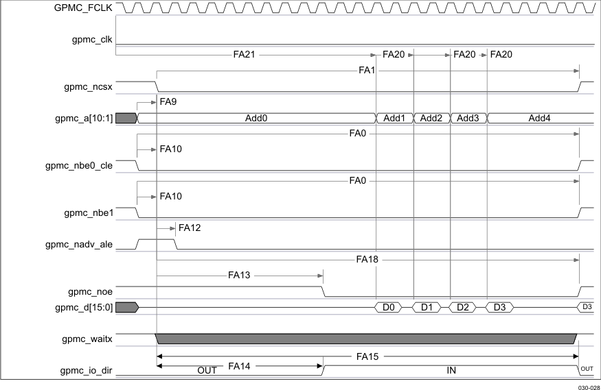
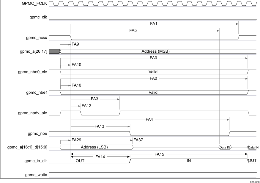
| FA5(1) | tacc(DAT) | Data maximum access time | H(5) | GPMC_FCLK cycles | |
| FA20(3) | tacc1-pgmode(DAT) | Page mode successive data maximum access time | P(4) | GPMC_FCLK cycles | |
| FA21(2) | tacc2-pgmode(DAT) | Page mode first data maximum access time | H(5) | GPMC_FCLK cycles | |
Table 6-8 GPMC/NOR Flash Interface Switching Characteristics – Asynchronous Mode
| NO. | PARAMETER | 1.8V/ 3.3V | UNIT | |||
|---|---|---|---|---|---|---|
| MIN | MAX | |||||
| tR(DO) | Rise time, output data | 2.0 | ns | |||
| tF(DO) | Fall time, output data | 2.0 | ns | |||
| FA0 | tW(nBEV) | Pulse duration, gpmc_nbe0_cle, gpmc_nbe1 valid time | Read | N(12) | ns | |
| Write | N(12) | ns | ||||
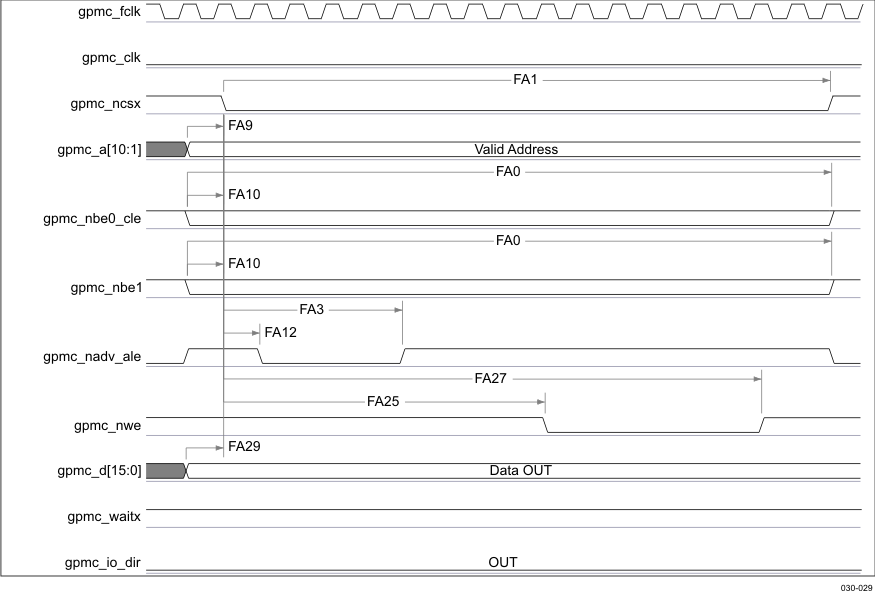
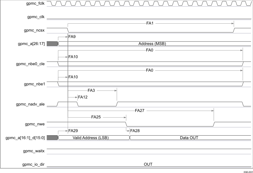
| FA1 | tW(nCSV) | Pulse duration, gpmc_ncsx(13) v low | Read | A(1) | ns | |
| Write | A(1) | ns | ||||
| FA3 | td(nCSV-nADVIV) | Delay time, gpmc_ncsx(13) valid to gpmc_nadv_ale invalid | Read | B(2) – 0.2 | B(2) + 2.0 | ns |
| Write | B(2) – 0.2 | B(2) + 2.0 | ns | |||
| FA4 | td(nCSV-nOEIV) | Delay time, gpmc_ncsx(13) valid to gpmc_noe invalid (Single read) | C(3) – 0.2 | C(3) + 2.0 | ns | |
| FA9 | td(AV-nCSV) | Delay time, address bus valid to gpmc_ncsx(13) valid | J(9) – 0.2 | J(9) + 2.0 | ns | |
| FA10 | td(nBEV-nCSV) | Delay time, gpmc_nbe0_cle, gpmc_nbe1 valid to gpmc_ncsx(13) valid | J(9) – 0.2 | J(9) + 2.0 | ns | |
| FA12 | td(nCSV-nADVV) | Delay time, gpmc_ncsx(13) valid to gpmc_nadv_ale valid | K(10) – 0.2 | K(10) + 2.0 | ns | |
| FA13 | td(nCSV-nOEV) | Delay time, gpmc_ncsx(13) valid to gpmc_noe valid | L(11) – 0.2 | L(11) + 2.0 | ns | |
| FA14 | td(nCSV-IODIR) | Delay time, gpmc_ncsx(13) valid to gpmc_io_dir high | L(11) – 0.2 | L(11) + 2.0 | ns | |
| FA15 | td(nCSV-IODIR) | Delay time, gpmc_ncsx(13) valid to gpmc_io_dir low | M(14) – 0.2 | M(14) + 2.0 | ns | |
| FA16 | tw(AIV) | Address invalid duration between 2 successive R/W accesses | G(7) | ns | ||
| FA18 | td(nCSV-nOEIV) | Delay time, gpmc_ncsx(13) valid to gpmc_noe invalid (Burst read) | I(8) – 0.2 | I(8) + 2.0 | ns | |
| FA20 | tw(AV) | Pulse duration, address valid – 2nd, 3rd, and 4th accesses | D(4) | ns | ||
| FA25 | td(nCSV-nWEV) | Delay time, gpmc_ncsx(13) valid to gpmc_nwe valid | E(5) – 0.2 | E(5) + 2.0 | ns | |
| FA27 | td(nCSV-nWEIV) | Delay time, gpmc_ncsx(13) valid to gpmc_nwe invalid | F(6) – 0.2 | F(6) + 2.0 | ns | |
| FA28 | td(nWEV-DV) | Delay time, gpmc_ new valid to data bus valid | 2.0 | ns | ||
| FA29 | td(DV-nCSV) | Delay time, data bus valid to gpmc_ncsx(13) valid | J(9) – 0.2 | J(9) + 2.0 | ns | |
| FA37 | td(nOEV-AIV) | Delay time, gpmc_noe valid to gpmc_a[16:1]_d[15:0] address phase end | 2.0 | ns | ||
-
For single read: A = (CSRdOffTime – CSOnTime) * (TimeParaGranularity + 1) * GPMC_FCLK
For single write: A = (CSWrOffTime – CSOnTime) * (TimeParaGranularity + 1) * GPMC_FCLK
For burst read: A = (CSRdOffTime – CSOnTime + (n – 1) * PageBurstAccessTime) * (TimeParaGranularity + 1) * GPMC_FCLK
For burst write: A = (CSWrOffTime – CSOnTime + (n – 1) * PageBurstAccessTime) * (TimeParaGranularity + 1) * GPMC_FCLK with n being the page burst access number -
For reading: B = ((ADVRdOffTime – CSOnTime) * (TimeParaGranularity + 1) + 0.5 * (ADVExtraDelay – CSExtraDelay)) * GPMC_FCLK
For writing: B = ((ADVWrOffTime – CSOnTime) * (TimeParaGranularity + 1) + 0.5 * (ADVExtraDelay – CSExtraDelay)) * GPMC_FCLK - C = ((OEOffTime – CSOnTime) * (TimeParaGranularity + 1) + 0.5 * (OEExtraDelay – CSExtraDelay)) * GPMC_FCLK
- D = PageBurstAccessTime * (TimeParaGranularity + 1) * GPMC_FCLK
- E = ((WEOnTime – CSOnTime) * (TimeParaGranularity + 1) + 0.5 * (WEExtraDelay – CSExtraDelay)) * GPMC_FCLK
- F = ((WEOffTime – CSOnTime) * (TimeParaGranularity + 1) + 0.5 * (WEExtraDelay – CSExtraDelay)) * GPMC_FCLK
- G = Cycle2CycleDelay * GPMC_FCLK
- I = ((OEOffTime + (n – 1) * PageBurstAccessTime – CSOnTime) * (TimeParaGranularity + 1) + 0.5 * (OEExtraDelay – CSExtraDelay)) * GPMC_FCLK
- J = (CSOnTime * (TimeParaGranularity + 1) + 0.5 * CSExtraDelay) * GPMC_FCLK
- K = ((ADVOnTime – CSOnTime) * (TimeParaGranularity + 1) + 0.5 * (ADVExtraDelay – CSExtraDelay)) * GPMC_FCLK
- L = ((OEOnTime – CSOnTime) * (TimeParaGranularity + 1) + 0.5 * (OEExtraDelay – CSExtraDelay)) * GPMC_FCLK
-
For single read: N = RdCycleTime * (TimeParaGranularity + 1) * GPMC_FCLK
For single write: N = WrCycleTime * (TimeParaGranularity + 1) * GPMC_FCLK
For burst read: N = (RdCycleTime + (n – 1) * PageBurstAccessTime) * (TimeParaGranularity + 1) * GPMC_FCLK
For burst write: N = (WrCycleTime + (n – 1) * PageBurstAccessTime) * (TimeParaGranularity + 1) * GPMC_FCLK - In gpmc_ncsx, x is equal to 0, 1, 2, 3, 4, 5, 6, or 7.
- M = ((RdCycleTime - CSOnTime) * (TimeParaGranularity + 1) - 0.5 * CSExtraDelay) * GPMC_FCLK
Above M parameter expression is given as one example of GPMC programming. IO DIR signal will go from IN to OUT after both RdCycleTime and BusTurnAround completion. Behavior of IO direction signal does depend on kind of successive Read/Write accesses performed to Memory and multiplexed or non-multiplexed memory addressing scheme, bus keeping feature enabled or not. IO DIR behavior is automatically handled by GPMC controller.
- In gpmc_ncsx, x is equal to 0, 1, 2, 3, 4, 5, 6, or 7. In gpmc_waitx, x is equal to 0, 1, 2, or 3.
- FA5 parameter provides amount of time required to internally sample input data. It is expressed in number of GPMC functional clock cycles. From start of read cycle and after FA5 functional clock cycles, input data is internally sampled by active functional clock edge. FA5 value must be stored inside AccessTime register bit field.
- GPMC_FCLK is an internal clock (GPMC functional clock) not provided externally.
- In gpmc_ncsx, x is equal to 0, 1, 2, 3, 4, 5, 6, or 7. In gpmc_waitx, x is equal to 0, 1, 2, or 3.
- FA21 parameter provides amount of time required to internally sample first input page data. It is expressed in number of GPMC functional clock cycles. From start of read cycle and after FA21 functional clock cycles, first input page data is internally sampled by active functional clock edge. FA21 value must be stored inside AccessTime register bit field.
- FA20 parameter provides amount of time required to internally sample successive input page data. It is expressed in number of GPMC functional clock cycles. After each access to input page data, next input page data is internally sampled by active functional clock edge after FA20 functional clock cycles. FA20 is also the duration of address phases for successive input page data (excluding first input page data). FA20 value must be stored in PageBurstAccessTime register bit field.
- GPMC_FCLK is an internal clock (GPMC functional clock) not provided externally.
- In gpmc_ncsx, x is equal to 0, 1, 2, 3, 4, 5, 6, or 7. In gpmc_waitx, x is equal to 0, 1, 2, or 3.
- FA5 parameter provides amount of time required to internally sample input data. It is expressed in number of GPMC functional clock cycles. From start of read cycle and after FA5 functional clock cycles, input data is internally sampled by active functional clock edge. FA5 value must be stored inside AccessTime register bit field.
- GPMC_FCLK is an internal clock (GPMC functional clock) not provided externally.
6.4.1.3 GPMC/NAND Flash Interface Timing
Table 6-9 through Table 6-12 assume testing over the recommended operating conditions and electrical characteristic conditions.
Table 6-9 GPMC/NAND Flash Asynchronous Mode Timing Conditions
| TIMING CONDITION PARAMETER | 1.8V, 3.3V | UNIT | ||
|---|---|---|---|---|
| MIN | MAX | |||
| Input Conditions | ||||
| tR | Input signal rise time | 1.8 | ns | |
| tF | Input signal fall time | 1.8 | ns | |
| CLOAD | Output load capacitance | 30 | pF | |
Table 6-10 GPMC/NAND Flash Interface Asynchronous Timing Internal Parameters(1)(2)
| NO. | PARAMETER | 1.8V, 3.3V | UNIT | |
|---|---|---|---|---|
| MIN | MAX | |||
| GNFI1 | Maximum output data generation delay from internal functional clock | 6.5 | ns | |
| GNFI2 | Maximum input data capture delay by internal functional clock | 4 | ns | |
| GNFI3 | Maximum device select generation delay from internal functional clock | 6.5 | ns | |
| GNFI4 | Maximum address latch enable generation delay from internal functional clock | 6.5 | ns | |
| GNFI5 | Maximum command latch enable generation delay from internal functional clock | 6.5 | ns | |
| GNFI6 | Maximum output enable generation delay from internal functional clock | 6.5 | ns | |
| GNFI7 | Maximum write enable generation delay from internal functional clock | 6.5 | ns | |
| GNFI8 | Maximum functional clock skew | 100 | ps | |
Table 6-11 GPMC/NAND Flash Interface Timing Requirements
| NO. | PARAMETER | 1.8V, 3.3V | UNIT | ||
|---|---|---|---|---|---|
| MIN | MAX | ||||
| GNF12(1) | tacc(DAT) | Data maximum access time | J(2) | GPMC_FCLK cycles | |
Table 6-12 GPMC/NAND Flash Interface Switching Characteristics
| NO. | PARAMETER | 1.8V, 3.3V | UNIT | ||
|---|---|---|---|---|---|
| MIN | MAX | ||||
| tR(DO) | Rise time, output data | 2.0 | ns | ||
| tF(DO) | Fall time, output data | 2.0 | ns | ||
| GNF0 | tw(nWEV) | Pulse duration, gpmc_nwe valid time | A(1) | ns | |
| GNF1 | td(nCSV-nWEV) | Delay time, gpmc_ncsx(13) valid to gpmc_nwe valid | B(2) - 0.2 | B(2) + 2.0 | ns |
| GNF2 | tw(CLEH-nWEV) | Delay time, gpmc_nbe0_cle high to gpmc_nwe valid | C(3) - 0.2 | C(3) + 2.0 | ns |
| GNF3 | tw(nWEV-DV) | Delay time, gpmc_d[15:0] valid to gpmc_nwe valid | D(4) - 0.2 | D(4) + 2.0 | ns |
| GNF4 | tw(nWEIV-DIV) | Delay time, gpmc_nwe invalid to gpmc_d[15:0] invalid | E(5) - 0.2 | E(5) + 2.0 | ns |
| GNF5 | tw(nWEIV-CLEIV) | Delay time, gpmc_nwe invalid to gpmc_nbe0_cle invalid | F(6) - 0.2 | F(6) + 2.0 | ns |
| GNF6 | tw(nWEIV-nCSIV) | Delay time, gpmc_nwe invalid to gpmc_ncsx(13) invalid | G(7) - 0.2 | G(7) + 2.0 | ns |
| GNF7 | tw(ALEH-nWEV) | Delay time, gpmc_nadv_ale High to gpmc_nwe valid | C(3) - 0.2 | C(3) + 2.0 | ns |
| GNF8 | tw(nWEIV-ALEIV) | Delay time, gpmc_nwe invalid to gpmc_nadv_ale invalid | F(6) - 0.2 | F(6) + 2.0 | ns |
| GNF9 | tc(nWE) | Cycle time, Write cycle time | H(8) | ns | |
| GNF10 | td(nCSV-nOEV) | Delay time, gpmc_ncsx(13) valid to gpmc_noe valid | I(9) - 0.2 | I(9) + 2.0 | ns |
| GNF13 | tw(nOEV) | Pulse duration, gpmc_noe valid time | K(10) | ns | |
| GN F14 | tc(nOE) | Cycle time, Read cycle time | L(11) | ns | |
| GNF15 | tw(nOEIV-nCSIV) | Delay time, gpmc_noe invalid to gpmc_ncsx(13) invalid | M(12) - 0.2 | M(12) + 2.0 | ns |
- A = (WEOffTime – WEOnTime) * (TimeParaGranularity + 1) * GPMC_FCLK
- B = ((WEOnTime – CSOnTime) * (TimeParaGranularity + 1) + 0.5 * (WEExtraDelay – CSExtraDelay)) * GPMC_FCLK
- C = ((WEOnTime – ADVOnTime) * (TimeParaGranularity + 1) + 0.5 * (WEExtraDelay – ADVExtraDelay)) * GPMC_FCLK
- D = (WEOnTime * (TimeParaGranularity + 1) + 0.5 * WEExtraDelay ) * GPMC_FCLK
- E = (WrCycleTime – WEOffTime * (TimeParaGranularity + 1) – 0.5 * WEExtraDelay ) * GPMC_FCLK
- F = (ADVWrOffTime – WEOffTime * (TimeParaGranularity + 1) + 0.5 * (ADVExtraDelay – WEExtraDelay ) * GPMC_FCLK
- G = (CSWrOffTime – WEOffTime * (TimeParaGranularity + 1) + 0.5 * (CSExtraDelay – WEExtraDelay ) * GPMC_FCLK
- H = WrCycleTime * (1 + TimeParaGranularity) * GPMC_FCLK
- I = ((OEOnTime – CSOnTime) * (TimeParaGranularity + 1) + 0.5 * (OEExtraDelay – CSExtraDelay)) * GPMC_FCLK
- K = (OEOffTime – OEOnTime) * (1 + TimeParaGranularity) * GPMC_FCLK
- L = RdCycleTime * (1 + TimeParaGranularity) * GPMC_FCLK
- M = (CSRdOffTime – OEOffTime * (TimeParaGranularity + 1) + 0.5 * (CSExtraDelay – OEExtraDelay ) * GPMC_FCLK
- In gpmc_ncsx, x is equal to 0, 1, 2, 3, 4, 5, 6, or 7.
- The GNF12 parameter provides amount of time required to internally sample input data. It is expressed in number of GPMC functional clock cycles. From start of read cycle and after GNF12 functional clock cycles, input data is internally sampled by active functional clock edge. The GNF12 value must be stored inside AccessTime register bit field.
- GPMC_FCLK is an internal clock (GPMC functional clock) not provided externally.
- In gpmc_ncsx, x is equal to 0, 1, 2, 3, 4, 5, 6, or 7. In gpmc_waitx, x is equal to 0 ,1, 2, or 3.
6.4.2 SDRAM Controller (SDRC)
The SDRC is a dedicated interface to DDR2/LPDDR1 SDRAM that performs the following functions:
- Buffering of input image data from sensors or video sources
- Intermediate buffering for processing/resizing of image data in the VPFE
- Numerous OSD display buffers
- Intermediate buffering for large raw Bayer data image files while performing image processing functions
- Buffering for intermediate data while performing video encode and decode functions
- Storage of executable code for the ARM
The main features of the controller are:
- Open Core Protocol 2.2 (OCP) compliant [7].
- Supports JEDEC standard compliant DDR2 [2] and LPDDR1 [4] devices.
- SDRAM address range over 2 chip selects.
- Supports following data bus widths:
- Supports following CAS latencies:
- Supports following number of internal banks:
- Supports 256, 512, 1024, and 2048-word page sizes.
- Supports following burst lengths:
- Supports sequential burst type.
- SDRAM auto initialization from reset or configuration change.
- Supports Bank Interleaving across both the chip selects.
- Supports Clock Stop mode for LPDDR1 for low power.
- Supports Self Refresh and Precharge Power-Down modes for low power.
- Supports Partial Array Self Refresh and Temperature Controlled Self Refresh modes for low power in LPDDR1.
- Temperature Controlled Self Refresh is only supported for mobile SDRAM having on-chip temperature sensor.
- Supports ODT on DDR2.
- Supports prioritized refresh.
- Programmable SDRAM refresh rate and backlog counter.
- Programmable SDRAM timing parameters.
- Supports only little endian.
OCP Data Bus Width SDRAM Data Bus Width 64 and 128-Bit 16, 32, and 64-Bit SDRAM Type CAS Latencies DDR2 2, 3, 4, 5, and 6 LPDDR1 2 and 3 SDRAM Type Internal Banks DDR2 1, 2, 4, and 8 LPDDR1 1, 2, and 4 SDRAM Type Burst Length DDR2 8 (4 not supported) LPDDR1 8 (2 and 4 not supported)
6.4.2.1 LPDDR Interface
This section provides the timing specification for the LPDDR interface as a PCB design and manufacturing specification. The design rules constrain PCB trace length, PCB trace skew, signal integrity, cross-talk, and signal timing. These rules, when followed, result in a reliable LPDDR memory system without the need for a complex timing closure process. For more information regarding guidelines for using this LPDDR specification, see the Understanding TI's PCB Routing Rule-Based DDR Timing Specification Application Report (SPRAAV0).
6.4.2.1.1 LPDDR Interface Schematic
Figure 6-17 and Figure 6-18 show the LPDDR interface schematics for a LPDDR memory system. The 1 x16 LPDDR system schematic is identical to Figure 6-17 except that the high word LPDDR device is deleted.
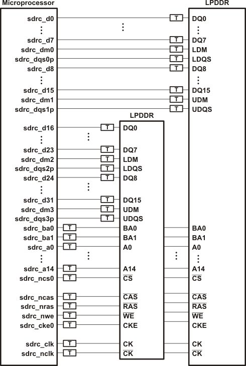 Figure 6-17 AM3517/05 LPDDR High Level Schematic (x16 memories)
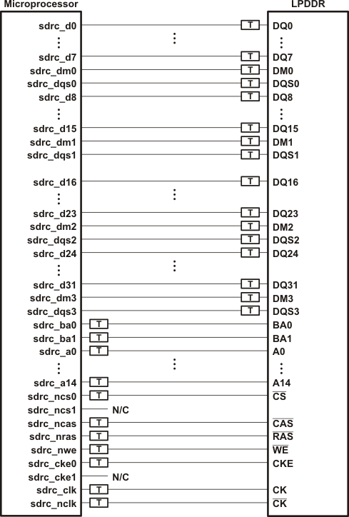 Figure 6-18 AM3517/05 LPDDR High Level Schematic (x32 memory)
6.4.2.1.2 Compatible JEDEC LPDDR Devices
Table 6-13 lists the parameters of the JEDEC LPDDR devices that are compatible with this interface. Generally, the LPDDR interface is compatible with x16 and x32 LPDDR333 speed grade LPDDR devices.
Table 6-13 Compatible JEDEC LPDDR Devices
| NO. | PARAMETER | MIN | MAX | UNIT | NOTES |
|---|---|---|---|---|---|
| 1 | JEDEC LPDDR Device Speed Grade | LPDDR333 | See Note (1) | ||
| 2 | JEDEC LPDDR Device Bit Width | 16 | 32 | Bits | |
| 3 | JEDEC LPDDR Device Count | 1 | 2 | Devices | See Note (2) |
| 4 | JEDEC LPDDR Device Ball Count | 60 | 90 | Balls |
6.4.2.1.3 PCB Stackup
The minimum stackup required for routing the microprocessor is a six layer stack as listed in Table 6-14. Additional layers may be added to the PCB stack up to accommodate other circuity or to reduce the size of the PCB footprint.
Table 6-14 Minimum PCB Stack Up
| LAYER | TYPE | DESCRIPTION |
|---|---|---|
| 1 | Signal | Top Routing Mostly Horizontal |
| 2 | Plane | Ground |
| 3 | Plane | Power |
| 4 | Signal | Internal Routing |
| 5 | Plane | Ground |
| 6 | Signal | Bottom Routing Mostly Vertical |
Table 6-15 PCB Stack Up Specifications
| NO. | PARAMETER | MIN | TYP | MAX | UNIT | NOTES |
|---|---|---|---|---|---|---|
| 1 | PCB Routing/Plane Layers | 6 | ||||
| 2 | Signal Routing Layers | 3 | ||||
| 3 | Full ground layers under LPDDR routing region | 2 | ||||
| 4 | Number of ground plane cuts allowed within LPDDR routing region | 0 | ||||
| 5 | Number of ground reference planes required for each LPDDR routing 1 layer | 1 | ||||
| 6 | Number of layers between LPDDR routing layer and reference ground 0 plane | 0 | ||||
| 7 | PCB Routing Feature Size | 4 | Mils | |||
| 8 | PCB Trace Width w | 4 | Mils | |||
| 9 | PCB BGA escape via pad size | 18 | Mils | |||
| 10 | PCB BGA escape via hole size | 8 | Mils | |||
| 11 | Device BGA Pad Size | See Note(1) | ||||
| 12 | LPDDR Device BGA Pad Size | See Note(2) | ||||
| 13 | Single Ended Impedance, ZO | 50 | 75 | Ω | ||
| 14 | Impedance Control | Z-5 | Z | Z + 5 | Ω | See Note(3) |
6.4.2.1.4 Placement
Figure 6-19 shows the required placement for the microprocessor as well as the LPDDR devices. The dimensions for Figure 6-19 are defined in Table 6-16. The placement does not restrict the side of the PCB that the devices are mounted on. The ultimate purpose of the placement is to limit the maximum trace lengths and allow for proper routing space. For 1x16 and 1x32 LPDDR memory systems, the second LPDDR device is omitted from the placement.
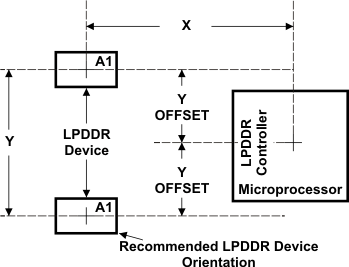 Figure 6-19 AM3517/05 and LPDDR Device Placement
Table 6-16 Placement Specifications
| NO. | PARAMETER | MIN | MAX | UNIT | NOTES |
|---|---|---|---|---|---|
| 1 | X | 1440 | Mils | See Notes(1), (2) | |
| 2 | Y | 1030 | Mils | See Notes(1), (2) | |
| 3 | Y Offset | 525 | Mils | See Notes(1),(2),(3) | |
| 4 | LPDDR Keepout Region | See Note(4) | |||
| 5 | Clearance from non-LPDDR signal to LPDDR Keepout Region | 4 | w | See Note(5) |
6.4.2.1.5 LPDDR Keep Out Region
The region of the PCB used for the LPDDR circuitry must be isolated from other signals. The LPDDR keep out region is defined for this purpose and is shown in Figure 6-20. The size of this region varies with the placement and LPDDR routing. Additional clearances required for the keep out region are listed in Table 6-16.
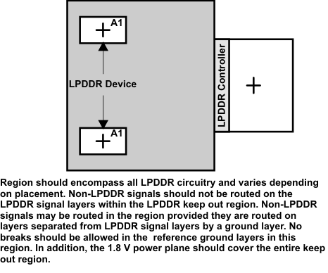 Figure 6-20 LPDDR Keepout Region
6.4.2.1.6 Net Classes
Table 6-17 lists the clock net classes for the LPDDR interface. Table 6-18 lists the signal net classes, and associated clock net classes, for the signals in the LPDDR interface. These net classes are used for the termination and routing rules that follow.
Table 6-17 Clock Net Class Definitions
| CLOCK NET CLASS | PIN NAMES |
|---|---|
| CK | sdrc_clk/sdrc_nclk |
| DQS0 | sdrc_dqs0 |
| DQS1 | sdrc_dqs1 |
| DQS2 | sdrc_dqs2 |
| DQS3 | sdrc_dqs3 |
Table 6-18 Signal Net Class Definitions
| CLOCK NET CLASS | ASSOCIATED CLOCK NET CLASS | PIN NAMES |
|---|---|---|
| ADDR_CTRL | CK | sdrc_ba, sdrc_a, sdrc_ncs0, sdrc_ncas, sdrc_nras, sdrc_nwe, sdrc_cke0 |
| DQ0 | DQS0 | sdrc_d, sdrc_dm0 |
| DQ1 | DQS1 | sdrc_d, sdrc_dm1 |
| DQ2 | DQS2 | sdrc_d, sdrc_dm2 |
| DQ3 | DQS3 | sdrc_d, sdrc_dm3 |
6.4.2.1.7 LPDDR Signal Termination
No terminations of any kind are required in order to meet signal integrity and overshoot requirements. Serial terminators are permitted, if desired, to reduce EMI risk; however, serial terminations are the only type permitted. Table 6-19 lists the specifications for the series terminators.
Table 6-19 LPDDR Signal Terminations
| NO. | PARAMETER | MIN | TYP | MAX | UNIT | NOTES |
|---|---|---|---|---|---|---|
| 1 | CK Net Class | 0 | 10 | Ω | See Note(1) | |
| 2 | ADDR_CTRL Net Class | 0 | 22 | Zo | Ω | See Notes(1),(2),(3) |
| 3 | Data Byte Net Classes (DQS0-DQS3, DQ0-DQ3) |
0 | 22 | Zo | Ω | See Notes(1),(2),(3) |
6.4.2.1.8 LPDDR CK and ADDR_CTRL Routing
Figure 6-21 shows the topology of the routing for the CK and ADDR_CTRL net classes. The route is a balanced T as it is intended that the length of segments B and C be equal. In addition, the length of A should be maximized.
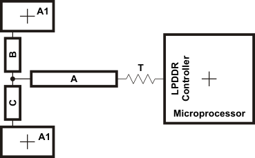 Figure 6-21 CK and ADDR_CTRL Routing and Topology
Table 6-20 CK and ADDR_CTRL Routing Specification
| NO. | PARAMETER | MIN | TYP | MAX | UNIT | NOTES |
|---|---|---|---|---|---|---|
| 1 | Center to Center CK-CK spacing | 2w | ||||
| 2 | CK A to B/A to C Skew Length Mismatch | 25 | Mils | See Note(1) | ||
| 3 | CK B to C Skew Length Mismatch | 25 | Mils | |||
| 4 | Center to Center CK to other LPDDR trace spacing |
4w | See Note(2) | |||
| 5 | CK/ADDR_CTRL nominal trace length | CACLM-50 | CACLM | CACLM+50 | Mils | See Note(3) |
| 6 | ADDR_CTRL to CK Skew Length Mismatch | 100 | Mils | |||
| 7 | ADDR_CTRL to ADDR_CTRL Skew Length Mismatch |
100 | Mils | |||
| 8 | Center to Center ADDR_CTRL to other LPDDR trace 4w spacing | 4w | See Note(2) | |||
| 9 | Center to Center ADDR_CTRL to other ADDR_CTRL 3w trace spacing | 3w | See Note(2) | |||
| 10 | ADDR_CTRL A to B/A to C Skew Length Mismatch | 100 | Mils | See Note(1) | ||
| 11 | ADDR_CTRL B to C Skew Length Mismatch | 100 | Mils |
Figure 6-22 shows the topology and routing for the DQS and DQ net classes; the routes are point to point. Skew matching across bytes is not needed nor recommended.
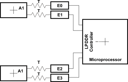 Figure 6-22 DQS and DQ Routing and Topology
Table 6-21 DQS and DQ Routing Specification(1)
| NO. | PARAMETER | MIN | TYP | MAX | UNIT | NOTES |
|---|---|---|---|---|---|---|
| 2 | DQS E Skew Length Mismatch | 25 | Mils | |||
| 3 | Center to Center DQS to other LPDDR trace spacing | 4w | See Note(2) | |||
| 4 | DQS/DQ nominal trace length | DQLM - 50 | DQLM | DQLM + 50 | Mils | See Note(2) |
| 5 | DQ to DQS Skew Length Mismatch | 100 | Mils | |||
| 6 | DQ to DQ Skew Length Mismatch | 100 | Mils | |||
| 7 | Center to Center DQ to other LPDDR trace spacing | 4w | See Note(2) | |||
| 8 | Center to Center DQ to other DQ trace spacing | 3w | See Note(2),(3) | |||
| 9 | DQ E Skew Length Mismatch | 100 | Mils |
6.4.2.2 DDR2 Interface
This section provides the timing specification for the DDR2 interface as a PCB design and manufacturing specification. The design rules constrain PCB trace length, PCB trace skew, signal integrity, cross-talk, and signal timing. These rules, when followed, result in a reliable DDR2 memory system without the need for a complex timing closure process. For more information regarding guidelines for using this DDR2 specification, Understanding TI's PCB Routing Rule-Based DDR2 Timing Specification (SPRAAV0).
6.4.2.2.1 DDR2 Interface Schematic
Figure 6-23 shows the DDR2 interface schematic for a dual-memory DDR2 system. The single-memory system is shown in Figure 6-24. Pin numbers for the AM3517/05 can be obtained from the pin description section.
6.4.2.2.2 Compatible JEDEC DDR2 Devices
Table 6-22 lists the parameters of the JEDEC DDR2 devices that are compatible with this interface. Generally, the DDR2 interface is compatible with x16 or x32 DDR2 speed grade DDR2-333 devices.
Table 6-22 Compatible JEDEC DDR2 Devices
| No. | Parameter | Min | Max | Unit | Notes |
|---|---|---|---|---|---|
| 1 | JEDEC DDR2 Device Speed Grade | DDR2-333 MHz | See Note (1) | ||
| 2 | JEDEC DDR2 Device Bit Width | x16 | x32 | Bits | |
| 3 | JEDEC DDR2 Device Count | 1 | 2 | Devices | See Note (3) |
| 4 | JEDEC DDR2 Device Ball Count | 84 | 92 | Balls | See Note (2) |
6.4.2.2.3 PCB Stackup
The minimum stackup required for routing the AM3517/05 is a six-layer stack as listed in Table 6-23. Additional layers may be added to the PCB stack up to accommodate other circuitry or to reduce the size of the PCB footprint.
Table 6-23 Minimum PCB Stack Up
| Layer | Type | Description |
|---|---|---|
| 1 | Signal | Top Routing Mostly Horizontal |
| 2 | Plane | Ground |
| 3 | Plane | Power |
| 4 | Signal | Internal Routing |
| 5 | Plane | Ground |
| 6 | Signal | Bottom Routing Mostly Vertical |
Complete stack up specifications are provided in Table 6-24.
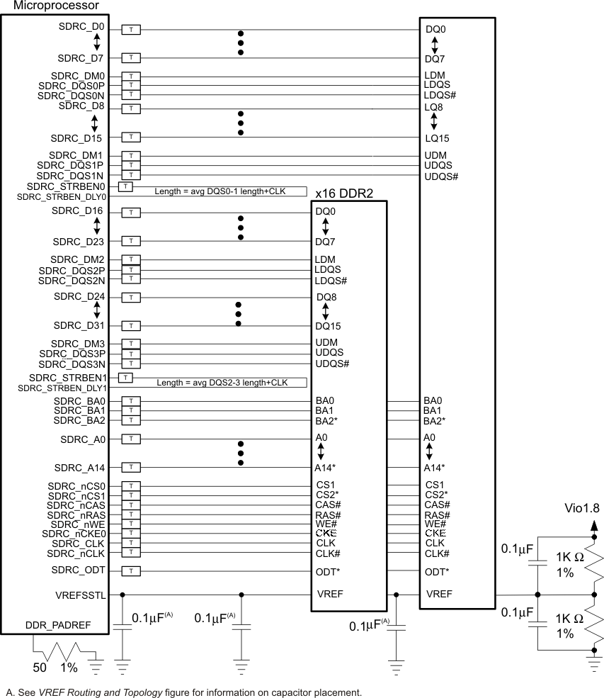 Figure 6-23 DDR2 Dual-Memory High Level Schematic
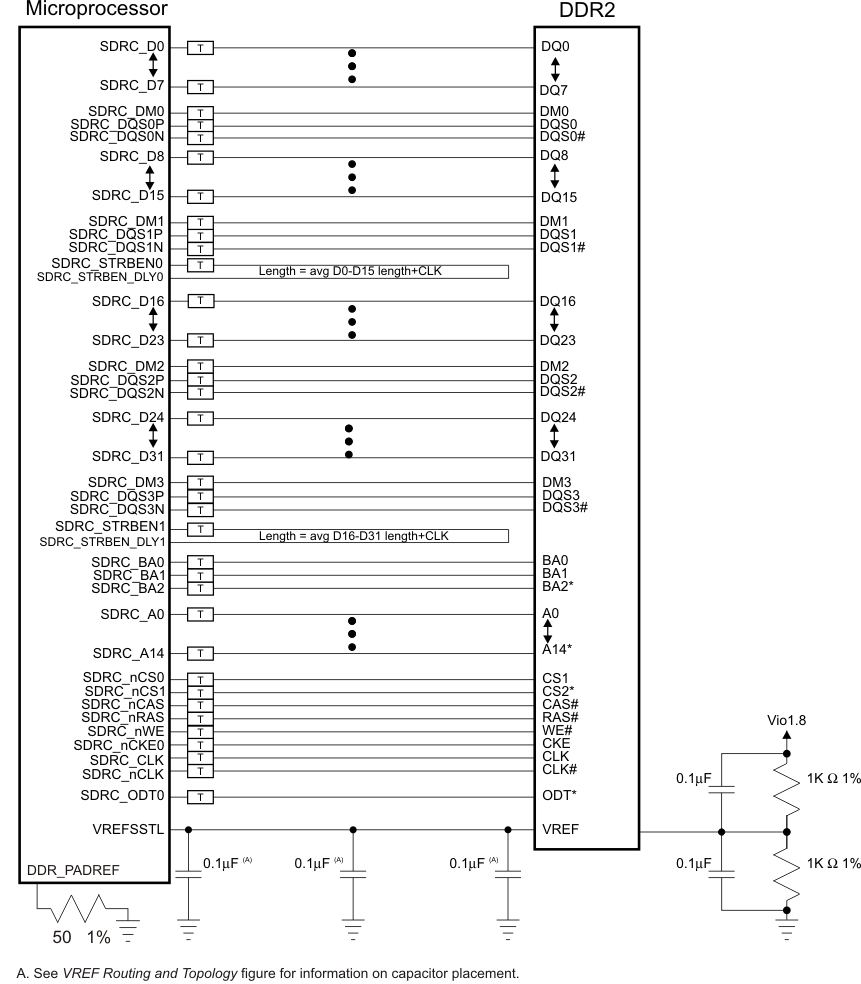 Figure 6-24 DDR2 Single-Memory High Level Schematic
Table 6-24 PCB Stack Up Specifications
| No. | Parameter | Min | Typ | Max | Unit | Notes |
|---|---|---|---|---|---|---|
| 1 | PCB Routing/Plane Layers | 6 | ||||
| 2 | Signal Routing Layers | 3 | ||||
| 3 | Full ground layers under DDR2 routing Region | 2 | ||||
| 4 | Number of ground plane cuts allowed within DDR routing region | 0 | ||||
| 5 | Number of ground reference planes required for each DDR2 routing layer | 1 | ||||
| 6 | Number of layers between DDR2 routing layer and ground plane | 0 | ||||
| 7 | PCB Routing Feature Size | 4 | Mils | |||
| 8 | PCB Trace Width w | 4 | Mils | |||
| 9 | PCB BGA escape via pad size | 20 | Mils | |||
| 10 | PCB BGA escape via hole size | 10 | Mils | |||
| 11 | AM3517/05 BGA pad size | 12 | See Note (1) | |||
| 12 | DDR2 Device BGA pad size | See Note (2) | ||||
| 13 | Single Ended Impedance, Zo | 50 | 75 | Ω | ||
| 14 | Impedance Control | Z-5 | Z | Z+5 | Ω | See Note (3) |
6.4.2.2.4 Placement
Figure 6-24 shows the required placement for the DDR2 devices. The dimensions for Figure 6-25 are defined in Table 6-25. The placement does not restrict the side of the PCB that the devices are mounted on. The ultimate purpose of the placement is to limit the maximum trace lengths and allow for proper routing space. For single-memory DDR2 systems, the second DDR2 device is omitted from the placement.
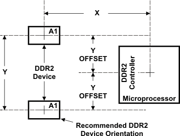 Figure 6-25 DDR2 Device Placement
Table 6-25 Placement Specifications
| No. | Parameter | Min | Max | Unit | Notes |
|---|---|---|---|---|---|
| 1 | X | 1750 | Mils | See Notes (1), (2) | |
| 2 | Y | 1280 | Mils | See Notes (1), (2) | |
| 3 | Y Offset | 650 | Mils | See Notes (1). (2), (3) | |
| 4 | DDR2 Keepout Region | See Note (4) | |||
| 5 | Clearance from non-DDR2 signal to DDR2 Keepout Region | 4 | w | See Note (5) |
6.4.2.2.5 DDR2 Keep Out Region
The region of the PCB used for the DDR2 circuitry must be isolated from other signals. The DDR2 keep out region is defined for this purpose and is shown in Figure 6-26. The size of this region varies with the placement and DDR routing. Additional clearances required for the keep out region are listed in Table 6-25.
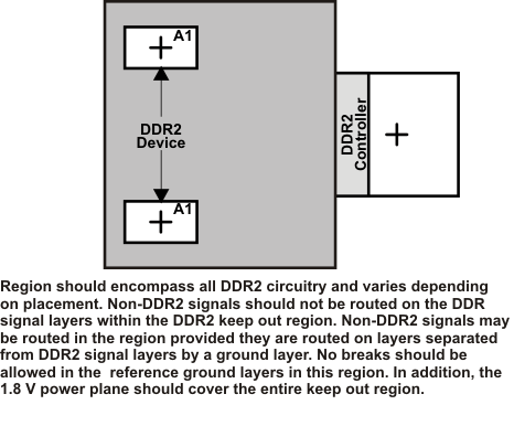 Figure 6-26 DDR2 Keepout Region
6.4.2.2.6 Bulk Bypass Capacitors
Bulk bypass capacitors are required for moderate speed bypassing of the DDR2 and other circuitry. Table 6-26 contains the minimum numbers and capacitance required for the bulk bypass capacitors. Note that this table only covers the bypass needs of the AM3517/05 and DDR2 interfaces. Additional bulk bypass capacitance may be needed for other circuitry.
Table 6-26 Bulk Bypass Capacitors
| No. | Parameter | Min | Max | Unit | Notes |
|---|---|---|---|---|---|
| 1 | VDDS Bulk Bypass Capacitor Count | 3 | Devices | See Note (1) | |
| 2 | VDDS Bulk Bypass Total Capacitance | 30 | uF | ||
| 3 | DDR#1 Bulk Bypass Capacitor Count | 1 | Devices | See Note (1) | |
| 4 | DDR#1 Bulk Bypass Total Capacitance | 22 | uF | ||
| 5 | DDR#2 Bulk Bypass Capacitor Count | 1 | Devices | See Notes (1), (2) | |
| 6 | DDR#2 Bulk Bypass Total Capacitance | 22 | uF | See Note (2) |
6.4.2.2.7 High-Speed Bypass Capacitors
High-speed (HS) bypass capacitors are critical for proper DDR2 interface operation. It is particularly important to minimize the parasitic series inductance of the HS bypass cap, AM3517/05 DDR2 power, and AM3517/05 DDR2 ground connections. Table 6-27 contains the specification for the HS bypass capacitors as well as for the power connections on the PCB.
6.4.2.2.8 Net Classes
Table 6-28 lists the clock net classes for the DDR2 interface. Table 6-29 lists the signal net classes, and associated clock net classes, for the signals in the DDR2 interface. These net classes are used for the termination and routing rules that follow.
Table 6-27 High-Speed Bypass Capacitors
| No. | Parameter | Min | Max | Unit | Notes |
|---|---|---|---|---|---|
| 1 | HS Bypass Capacitor Package Size | 0402 | 10 Mils | See Note (1) | |
| 2 | Distance from HS bypass capacitor to device being bypassed | 250 | Mils | ||
| 3 | Number of connection vias for each HS bypass capacitor | 2 | Vias | See Note (4) | |
| 4 | Trace length from bypass capacitor contact to connection via | 1 | 30 | Mils | |
| 5 | Number of connection vias for each DDR2 device power or ground balls | 1 | Vias | ||
| 6 | Trace length from DDR2 device power ball to connection via | 35 | Mils | ||
| 7 | VDDS HS Bypass Capacitor Count | 20 | Devices | See Note (2) | |
| 8 | VDDS HS Bypass Capacitor Total Capacitance | 1.2 | μF | ||
| 9 | DDR#1 HS Bypass Capacitor Count | 8 | Devices | See Note (2) | |
| 10 | DDR#1 HS Bypass Capacitor Total Capacitance | 0.4 | μF | ||
| 11 | DDR#2 HS Bypass Capacitor Count | 8 | Devices | See Notes (2), (3) | |
| 12 | DDR#2 HS Bypass Capacitor Total Capacitance | 0.4 | μF | See Note (3) |
Table 6-28 Clock Net Class Definitions
| Clock Net Class | AM3517/05 Device Pin Names |
|---|---|
| CK | sdrc_clk/sdrc_nclk |
| DQS0 | sdrc_dqs0p /sdrc_dqs0n |
| DQS1 | sdrc_dqs1p /sdrc_dqs1n |
| DQS2 | sdrc_dqs2p/sdrc_dqs2n |
| DQS3 | sdrc_dqs3p/sdrc_dqs3n |
Table 6-29 Signal Net Class Definitions
| Clock Net Class | Associated Clock Net Class | AM3517/05 Device Pin Names |
|---|---|---|
| ADDR_CTRL | CK | sdrc_ba[2:0], sdrc_ncs1, sdrc_a[14:0], sdrc_ncs0 , sdrc_ncas, sdrc_nras, sdrc_nwe, sdrc_cke0 |
| DQ0 | DQS0 | sdrc_d[7:0], sdrc_dm0 |
| DQ1 | DQS1 | sdrc_d[15:8], sdrc_dm1 |
| DQ2 | DQS2 | sdrc_d[23:16],sdrc_dm2 |
| DQ3 | DQS3 | sdrc_d[31:24],sdrc_dm3 |
| SDRC_STRBEN0 | CK,DQS0,DQS1 | sdrc_strben0, sdrc_strben_dly0 |
| SDRC_STRBEN1 | CK,DQS2,DQS3 | sdrc_strben1, sdrc_strben_dly1 |
6.4.2.2.9 DDR2 Signal Termination
No terminations of any kind are required in order to meet signal integrity and overshoot requirements. Serial terminators are permitted, if desired, to reduce EMI risk; however, serial terminations are the only type permitted. Table 6-30 lists the specifications for the series terminators.
Table 6-30 DDR2 Signal Terminations
| No. | Parameter | Min | Typ | Max | Unit | Notes |
|---|---|---|---|---|---|---|
| 1 | CLK Net Class | 0 | 10 | Ω | See Note (1) | |
| 2 | ADDR_CTRL Net Class | 0 | 22 | Zo | Ω | See Notes (1), (2), (3) |
| 3 | Data Byte Net Classes (DQS0-DQS1, D0-D31) | 0 | 22 | Zo | Ω | See Notes (1), (2), (3) |
| 4 | SDRC_STRBENx Net Class (SDRC_STRBENx) | 0 | 10 | Zo | Ω | See Notes (1), (2), (3) |
6.4.2.2.10 VREF Routing
VREF is used as a reference by the input buffers of the DDR2 memories as well as the AM3517/05. VREF is intended to be half of the DDR2 power supply voltage and should be created using a resistive divider as shown in Figure 6-23. Other methods of creating VREF are not recommended. Figure 6-27 shows the layout guidelines for VREF.
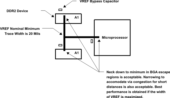 Figure 6-27 VREF Routing and Topology
6.4.2.2.11 DDR2 CLK and ADDR_CTRL Routing
Figure 6-28 shows the topology of the routing for the CLK and ADDR_CTRL net classes. The route is a balanced T as it is intended that the length of segments B and C be equal. In addition, the length of A should be maximized.
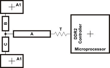 Figure 6-28 CLK and ADDR_CTRL Routing and Topology
Table 6-31 CLK and ADDR_CTRL Routing Specification (1)
| No | Parameter | Min | Typ | Max | Unit | Notes |
|---|---|---|---|---|---|---|
| 1 | Center to center DQS-DQSN spacing | 2w | ||||
| 2 | CK differential pair Skew Length Mismatch(4) | 25 | Mils | See Note (1) | ||
| 3 | CLKB to CLKC Skew Length Mismatch | 25 | Mils | |||
| 4 | Center to center CLK to other DDR2 trace spacing | 4w | See Note (3) | |||
| 5 | CK/ADDR_CTRL nominal trace length | CACLM-50 | CACLM | CACLM+50 | Mils | See Note (2) |
| 6 | ADDR_CTRL to CLK Skew Length Mismatch | 100 | Mils | |||
| 7 | ADDR_CTRL to ADDR_CTRL Skew Length Mismatch | 100 | Mils | |||
| 8 | Center to center ADDR_CTRL to other DDR2 trace spacing | 4w | See Note (3) | |||
| 9 | Center to center ADDR_CTRL to other ADDR_CTRL trace spacing | 3w | See Note (3) | |||
| 10 | ADDR_CTRL A to B, ADDR_CTRL A to C, Skew Length Mismatch | 100 | Mils | See Note (1) | ||
| 11 | ADDR_CTRL B to C Skew Length Mismatch | 100 | Mils |
Figure 6-29 shows the topology and routing for the DQS and Dx net classes; the routes are point to point. Skew matching across bytes is not needed nor recommended.
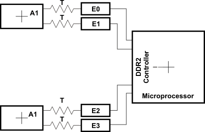 Figure 6-29 DQS and Dx Routing and Topology
Table 6-32 DQS and Dx Routing Specification(6)(1)
| No. | Parameter | Min | Typ | Max | Unit | Notes |
|---|---|---|---|---|---|---|
| 1 | Center to center DQS-DQSN spacing | 2w | ||||
| 2 | DQS E differential pair Skew Length Mismatch(7) | 25 | Mils | |||
| 3 | Center to center DQS to other DDR2 trace spacing | 4w | See Note (4) | |||
| 4 | DQS/Dx nominal trace length | DQLM-50 | DQLM | DQLM+50 | Mils | See Notes (1), (3) |
| 5 | Dx to DQS Skew Length Mismatch | 100 | Mils | See Note (3) | ||
| 6 | Dx to Dx Skew Length Mismatch | 100 | Mils | See Note (3) | ||
| 7 | Center to center Dx to other DDR2 trace spacing | 4w | See Notes (4), (5) | |||
| 8 | Center to Center Dx to other Dx trace spacing | 3w | See Notes (2), (4) |
Figure 6-30 shows the routing for the SDRC_STRBENx net classes. Table 6-33 contains the routing specification. SDRC_STRBENx net classes should be shielded from or routed on different layers than the DQx net classes.
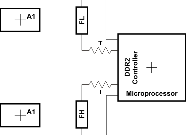 Figure 6-30 SDRC_STRBENx Routing
Table 6-33 SDRC_STRBENx Routing Specification(4)(5)
| No. | Parameter | Min | Typ | Max | Unit | Notes |
|---|---|---|---|---|---|---|
| 1 | SDRC_STRBEN0 Length F | CKB0B1 | See Note (1) | |||
| SDRC_STRBEN1 Length F | CKB0B2 | See Note (2) | ||||
| 3 | Center to center SDRC_STRBENx to any other trace spacing | 4w | ||||
| 4 | DQS/Dx nominal trace length | DQLM-50 | DQLM | DQLM+50 | Mils | |
| 5 | SDRC_STRBENx Skew | 100 | Mils | See Note (3) |
6.4.2.2.12 On Die Termination (ODT)
ODT should only be used with 1 chip select as shown in Figure 6-31. If using sdrc_cs0 and sdrc_cs1, sdrc_odt should not be used. ODT signals should be tied off at the memory.
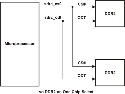 Figure 6-31 ODT Connection Using One Chip select (sdrc_cs0)
6.5 Video Interfaces
6.5.1 Video Processing Subsystem (VPSS)
The Video Processing Sub-System (VPSS) provides a Video Processing Front End (VPFE) input interface for external imaging peripherals (i.e., image sensors, video decoders, and so forth).
6.5.1.1 Video Processing Front End (VPFE)
The Video Processing Front-End (VPFE) controller receives input video/image data from external capture devices and stores it to external memory which is transferred into the external memory via a built in DMA engine. An internal buffer block provides a high bandwidth path between the VPSS module and the external memory. The Cortex-A8 will process the image data based on application requirements.
6.5.1.1.1 Video Processing Front End (VPFE) Timing
Table 6-34 and Table 6-35 assume testing over recommended operating conditions.
Table 6-34 VPFE Timing Requirements
| NO. | PARAMETER | 1.8V, 3.3V | |||
|---|---|---|---|---|---|
| MIN | MAX | UNIT | |||
| VF1 | tc(VDIN_CLK) | Cycle time, pixel clock input, VDIN_CLK | 13.33 | 100 | ns |
| VF2 | tsu(VDIN_D-VDIN_CLK) | Setup time, VDIN_D to VDIN_CLK rising edge | 3.5 | ns | |
| VF3 | tsu(VDIN_HD-VDIN_CLK) | Setup time, VDIN_HD to VDIN_CLK rising edge | 3.5 | ns | |
| VF4 | tsu(VDIN_VD-VDIN_CLK) | Setup time, VDIN_VD to VDIN_CLK rising edge | 3.5 | ns | |
| VF5 | tsu(VDIN_WEN-VDIN_CLK) | Setup time, VDIN_WEN to VDIN_CLK rising edge | 3.5 | ns | |
| VF6 | tsu(C_FLD-VDIN_CLK) | Setup time, VDIN_FIELD to VDIN_CLK rising edge | 3.5 | ns | |
| VF7 | th(VDIN_CLK-VDIN_D) | Hold time, VDIN_D valid after VDIN_CLK rising edge | 2.5 | ns | |
| VF8 | th(VDIN-HD-VDIN_CLK) | Hold time, VDIN_HD to VDIN_CLK rising edge | 2.5 | ns | |
| VF9 | th(VDIN_VD-VDIN_CLK) | Hold time, VDIN_VD to VDIN_CLK rising edge | 2.5 | ns | |
| VF10 | th(VDIN_WEN-VDIN_CLK) | Hold time, VDIN_WEN to VDIN_CLK rising edge | 2.5 | ns | |
| VF11 | th(C_FLD-VDIN_CLK) | Hold time, VDIN_FIELD to VDIN_CLK rising edge | 2.5 | ns | |
Table 6-35 VPFE Output Switching Characteristics
| NO. | PARAMETER | 1.8V, 3.3V | |||
|---|---|---|---|---|---|
| MIN | MAX | UNIT | |||
| VF12 | td(VDIN_HD-VDIN_CLK) | Output delay time, VDIN_HD to CLK rising edge | 10 | ns | |
| VF13 | td(VDIN_VD-VDIN_CLK) | Output delay time, VDIN_VD to CLK rising edge | 10 | ns | |
| VF14 | td(VDIN_WEN-VDIN_CLK) | Output delay time, VDIN_WEN to CLK rising edge | 10 | ns | |
| VF15 | toh(VDIN_HD-VDIN_CLK) | Output hold time, VDIN_HD to CLK rising edge | 0.5 | ns | |
| VF16 | toh(VDIN_VD-VDIN_CLK) | Output hold time, VDIN_VD to CLK rising edge | 0.5 | ns | |
| VF17 | toh(C_FLD-VDIN_CLK) | Output hold time, VDIN_FLD to CLK rising edge | 0.5 | ns | |
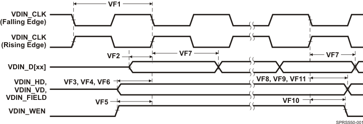 Figure 6-32 VPFE0 Input Timings
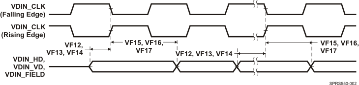 Figure 6-33 VPFE Output Timings
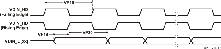 Figure 6-34 VPFE Input Timings With VDIN0_HD as Pixel Clock
6.5.2 Display Subsystem (DSS)
The display subsystem (DSS) provides the logic to display the video frame from external (SDRAM) or internal (SRAM) memory on an LCD panel or a TV set. The DSS integrates a display controller. It can be used in two configurations:
- LCD display support in:
- Bypass mode (RFBI module bypassed)
- RFBI mode (through RFBI module)
- TV display support (not discussed in this document because of its analog IO signals)
The two display supports can be active at the same time.
6.5.2.1 LCD Display Support in Bypass Mode
Two types of LCD panel are supported:
- Thin film transistor (TFT) or active matrix technology
- Supertwisted nematic (STN) or passive matrix technology
Both configurations are discussed in the following paragraphs.
6.5.2.1.1 LCD Display in TFT Mode
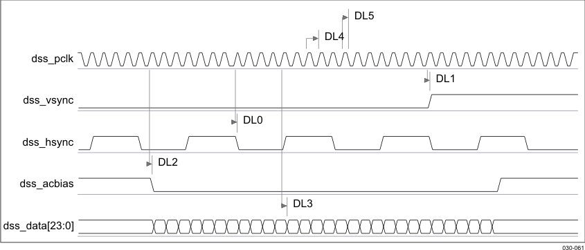
Table 6-36 assumes testing over the recommended operating conditions (see Figure 6-35).
Table 6-36 LCD Display Interface Switching Characteristics in TFT Mode(2)
| NO. | PARAMETER | 1.8V, 3.3V | UNIT | ||
|---|---|---|---|---|---|
| MIN | MAX | ||||
| DL0 | td(PCLKA-HSYNCT) | Delay time, dss_pclk active edge to dss_hsync transition | -4.215 | 4.215 | ns |
| DL1 | td(PCLKA-VSYNCT) | Delay time, dss_pclk active edge to dss_vsync transition | -4.215 | 4.215 | ns |
| DL2 | td(PCLKA-ACBIASA) | Delay time, dss_pclk active edge to dss_acbias active level | -4.215 | 4.215 | ns |
| DL3 | td(PCLKA-DATAV) | Delay time, dss_pclk active edge to dss_data bus valid | -4.215 | 4.215 | ns |
| DL4 | tc(PCLK) | Cycle time(1), dss_pclk | 13.468 | ns | |
| DL5 | tw(PCLK) | Pulse duration, dss_pclk low or high | 6.06 | 7.46 | ns |
| cload | Load capacitance | 25 | pF | ||
- The pixel data bus depends on the use of 8-, 9-, 12-, 16-, 18-, or 24-bit per pixel data output pins.
- The pixel clock frequency is programmable.
- All timings not illustrated in the waveform are programmable by software, control signal polarity, and driven edge of dss_pclk.
- For more information, see the AM35x ARM Microprocessor Technical Reference Manual (SPRUGR0).
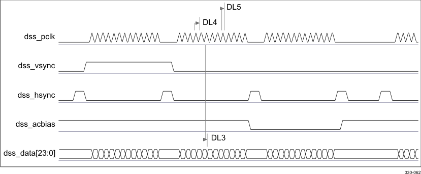
6.5.2.1.2 LCD Display in STN Mode
Table 6-37 assumes testing over the recommended operating conditions (see Figure 6-36).
Table 6-37 LCD Display Interface Switching Characteristics in STN Mode(2)(3)(4)
| NO. | PARAMETER | 1.8V, 3.3V | UNIT | ||
|---|---|---|---|---|---|
| MIN | MAX | ||||
| DL3 | td(PCLKA-DATAV) | Delay time, dss_pclk active edge to dss_data bus valid | -4.21 | 6.9 | ns |
| DL4 | tc(PCLK) | Cycle time(1), dss_pclk | 22.73 | ns | |
| DL5 | tw(PCLK) | Pulse duration, dss_pclk low or high | 10.23 | 12.5 | ns |
| cload | Load capacitance | 40 | pF | ||
- The pixel data bus depends on the use 4-, 8-, 12-, 16-, 18-, or 24-bit per pixel data output pins.
- All timings not illustrated in the waveform are programmable by software, control signal polarity, and driven edge of dss_pclk.
- dss_vsync width must be programmed to be as small as possible.
- The pixel clock frequency is programmable.
- For more information, see the AM35x ARM Microprocessor Technical Reference Manual (SPRUGR0).
6.6 Serial Communications Interfaces
6.6.1 Multichannel Buffered Serial Port (McBSP) Timing
There are five McBSP modules called McBSP1 through McBSP5. McBSP provides a full-duplex, direct serial interface between the AM3517/05 device and other devices in a system such as other application devices or codecs. It can accommodate a wide range of peripherals and clocked frame-oriented protocols (I2S, PCM, and TDM) due to its high level of versatility.
The McBSP1-5 modules may support two types of data transfer at the system level:
- The full-cycle mode, for which one clock period is used to transfer the data, generated on one edge and captured on the same edge (one clock period later).
- The half-cycle mode, for which one half clock period is used to transfer the data, generated on one edge and captured on the opposite edge (one half clock period later). Note that a new data is generated only every clock period, which secures the required hold time.
The interface clock (CLKX/CLKR) activation edge (data/frame sync capture and generation) has to be configured accordingly with the external peripheral (activation edge capability) and the type of data transfer required at the system level.
The AM3517/05 McBSP1-5 timing characteristics are described for both rising and falling activation edges. McBSP1 supports:
- 6-pin mode: dx and dr as data pins; clkx, clkr, fsx, and fsr as control pins.
- 4-pin mode: dx and dr as data pins; clkx and fsx pins as control pins. The clkx and fsx pins are internally looped back via software configuration, respectively, to the clkr and fsr internal signals for data receive.
McBSP2, 3, 4, and 5 support only the 4-pin mode.
The following sections describe the timing characteristics for applications in normal mode (that is, AM3517/05 McBSPx connected to one peripheral) and TDM applications in multipoint mode.
6.6.1.1 McBSP in Normal Mode
Table 6-38 through Table 6-40 assume testing over the recommended operating conditions.
Table 6-38 McBSP Timing Conditions
| TIMING CONDITION PARAMETER | 1.8V, 3.3 V | UNIT | ||
|---|---|---|---|---|
| Input Conditions | VALUE | |||
| tR | Input signal rise time | 2(1) | ns | |
| tF | Input signal fall time | 2 | ns | |
| Output Conditions | ||||
| CLOAD | Output load capacitance | 10 | pF | |
Table 6-39 McBSP1,2,4,5 Output Clock Pulse Duration
| PARAMETER | VDDSHV = 1.8V, 3.3V | UNIT | ||
|---|---|---|---|---|
| MIN | MAX | |||
| tC(CLK) | Cycle Time, mcbsp1_clkr/mcbspx_clkx(2) | 20.83 | ns | |
| tW(CLKH) | Typical pulse duration, mcbsp1_clkr / mcbspx_clkx high(2) | 0.5*P(1) | 0.5*P(1) | ns |
| tW(CLKL) | Typical pulse duration, mcbsp1_clkr / mcbspx_clkx low(2) | 0.5*P(1) | 0.5*P(1) | ns |
| tdc(CLK) | Duty cycle error, mcbsp1_clkr / mcbspx_clkx(2) | -0.75 | 0.75 | ns |
Table 6-40 McBSP3 Output Clock Pulse Duration
| PARAMETER | VDDSHV = 1.8V, 3.3V | UNIT | ||
|---|---|---|---|---|
| MIN | MAX | |||
| tC(CLK) | Cycle time, mcbsp3_clkx | 31.25 | ns | |
| tW(CLKH) | Typical pulse duration, mcbsp3_clkx high | 0.5*P(1) | 0.5*P(1) | ns |
| tW(CLKL) | Typical pulse duration, mcbsp3_clkx low | 0.5*P(1) | 0.5*P(1) | ns |
| tdc(CLK) | Duty cycle error, mcbsp3_clkx | -0.75 | 0.75 | ns |
6.6.1.1.1 McBSP1
Table 6-41 through Table 6-48 list the timing requirements and switching characteristics for McBSP1.
Table 6-41 McBSP1 Timing Requirements - Rising Edge and Receive Mode
| No. | PARAMETER | VDDSHV=3.3V | VDDSHV=1.8V | UNIT | ||||
|---|---|---|---|---|---|---|---|---|
| MIN | MAX | MIN | MAX | |||||
| B3 | tsu(DRV-CLKAE) | Setup time, mcbsp1_dr valid before mcbsp1_clkr / mcbsp1_clkx active edge | Half Cycle Master | 5.0 | 5.0 | ns | ||
| Half Cycle Slave | 5.2 | 5.2 | ns | |||||
| Full Cycle Master | 4.0 | 4.0 | ns | |||||
| Full Cycle Slave | 4.2 | 4.2 | ns | |||||
| B4 | th(CLKAE-DRV) | Hold time, mcbsp1_dr valid after mcbsp1_clkr / mcbsp1_clkx active edge | Half Cycle Master | 5.8 | 5.8 | ns | ||
| Half Cycle Slave | 5.2 | 5.2 | ns | |||||
| Full Cycle Master | 1.5 | 1.5 | ns | |||||
| Full Cycle Slave | 0.9 | 0.9 | ns | |||||
| B5 | tsu(FSV-CLKAE) | Setup time, mcbsp1_fsr / mcbsp1_fsx valid before mcbsp1_clkr / mcbsp1_clkx active edge | Half Cycle Slave | 5.2 | 5.2 | ns | ||
| Full Cycle Slave | 4.2 | 4.2 | ns | |||||
| B6 | th(CLKAE-FSV) | Hold time, mcbsp1_fsr / mcbsp1_fsx valid after mcbsp1_clkr / mcbsp1_clkx active edge | Half Cycle Slave | 0.5 | 0.5 | ns | ||
| Full Cycle Slave | 1.0 | 1.0 | ns | |||||
Table 6-42 McBSP1 Switching Characteristics - Rising Edge and Receive Mode
| No. | PARAMETER | VDDSHV=3.3V | VDDSHV=1.8V | UNIT | ||||
|---|---|---|---|---|---|---|---|---|
| MIN | MAX | MIN | MAX | |||||
| B2 | td(CLKAE-FSV) | Delay time, mcbsp1_clkr active edge to mcbsp1_fsr / mcbsp1_fsx valid | 0.2 | 14.8 | 0.2 | 14.8 | ns | |
Table 6-43 McBSP1 Timing Requirements - Rising Edge and Transmit Mode
| No. | PARAMETER | VDDSHV = 3.3V | VDDSHV = 1.8V | UNIT | ||||
|---|---|---|---|---|---|---|---|---|
| MIN | MAX | MIN | MAX | |||||
| B5 | tsu(FSXV-CLKXAE) | Setup time, mcbsp1_fsx valid before mcbsp1_clkx active edge | Full Cycle Slave | 5.2 | 4.7 | ns | ||
| Half Cycle Slave | 4.2 | 3.7 | ns | |||||
| B6 | th(CLKXAE-FSXV) | Hold time, mcbsp1_fsx valid after mcbsp1_clkx active edge | Full Cycle Slave | 5.2 | 4.7 | ns | ||
| Half Cycle Slave | 1.0 | 0.5 | ns | |||||
Table 6-44 McBSP1 Switching Characteristics - Rising Edge and Transmit Mode
| No. | PARAMETER | VDDSHV = 3.3V | VDDSHV = 1.8V | UNIT | ||||
|---|---|---|---|---|---|---|---|---|
| MIN | MAX | MIN | MAX | |||||
| B2 | td(CLKXAE-FSXV) | Delay time, mcbsp1_clkx active edge to mcbsp1_fsx valid | 0.2 | 14.8 | 0.7 | 14.8 | ns | |
| B8 | td(CLKXAE-DXV) | Delay time, mcbsp1_clkx active edge to mcbsp1_dx valid | Master | 0.6 | 14.8 | 0.6 | 14.8 | ns |
| Slave | 0.6 | 14.8 | 0.6 | 14.8 | ns | |||
Table 6-45 McBSP1 Timing Requirements - Falling Edge and Receive Mode
| No. | PARAMETER | VDDSHV = 3.3V | VDDSHV = 1.8V | UNIT | ||||
|---|---|---|---|---|---|---|---|---|
| MIN | MAX | MIN | MAX | |||||
| B3 | tsu(DRV-CLKAE) | Setup time, mcbsp1_dr valid before mcbsp1_clkr / mcbsp1_clkx active edge | Half Cycle Master | 5.0 | 5.0 | ns | ||
| Half Cycle Slave | 5.2 | 5.2 | ns | |||||
| Full Cycle Master | 4.0 | 4.0 | ns | |||||
| Full Cycle Slave | 4.2 | 4.2 | ns | |||||
| B4 | th(CLKAE-DRV) | Hold time, mcbsp1_dr valid after mcbsp1_clkr / mcbsp1_clkx active edge | Half Cycle Master | 5.8 | 5.8 | ns | ||
| Half Cycle Slave | 5.2 | 5.2 | ns | |||||
| Full Cycle Master | 1.5 | 1.5 | ns | |||||
| Full Cycle Slave | 0.9 | 0.9 | ns | |||||
| B5 | tsu(FSV-CLKAE) | Setup time, mcbsp1_fsr / mcbsp1_fsx valid before mcbsp1_clkr / mcbsp1_clkx active edge | Half Cycle Slave | 5.2 | 5.2 | ns | ||
| Full Cycle Slave | 4.2 | 4.2 | ns | |||||
| B6 | th(CLKAE-FSV) | Hold time, mcbsp1_fsr / mcbsp1_fsx valid after mcbsp1_clkr / mcbsp1_clkx active edge | Half Cycle Slave | 0.5 | 0.5 | ns | ||
| Full Cycle Slave | 1.0 | 1.0 | ns | |||||
Table 6-46 McBSP1 Switching Characteristics - Falling Edge and Receive Mode
| No. | PARAMETER | VDDSHV = 3.3V | VDDSHV = 1.8V | UNIT | ||||
|---|---|---|---|---|---|---|---|---|
| MIN | MAX | MIN | MAX | |||||
| B2 | td(CLKAE-FSV) | Delay time, mcbsp1_clkr / mcbsp1_clkx active edge to mcbsp1_fsr / mcbsp1_fsx valid | 0.2 | 14.8 | 0.7 | 14.8 | ns | |
Table 6-47 McBSP1 Timing Requirements - Falling Edge and Transmit Mode
| No. | PARAMETER | VDDSHV = 3.3V | VDDSHV = 1.8V | UNIT | ||||
|---|---|---|---|---|---|---|---|---|
| MIN | MAX | MIN | MAX | |||||
| B5 | tsu(FSXV-CLKXAE) | Setup time, mcbsp1_fsx valid before mcbsp1_clkx active edge | Half Cycle Slave | 5.2 | 5.2 | ns | ||
| Full Cycle Slave | 4.2 | 4.2 | ns | |||||
| B6 | th(CLKXAE-FSXV) | Hold time, mcbsp1_fsx valid after mcbsp1_clkx active edge | Half Cycle Slave | 5.2 | 5.2 | ns | ||
| Full Cycle Slave | 1.0 | 1.0 | ns | |||||
Table 6-48 McBSP1 Switching Characteristics - Falling Edge and Transmit Mode
| No. | PARAMETER | VDDSHV = 3.3V | VDDSHV = 1.8V | UNIT | ||||
|---|---|---|---|---|---|---|---|---|
| MIN | MAX | MIN | MAX | |||||
| B2 | td(CLKXAE-FSXV) | Delay time, mcbsp1_clkx active edge to mcbsp1_fsx valid | 0.2 | 14.8 | 0.2 | 14.8 | ns | |
| B8 | td(CLKXAE-DXV) | Delay time, mcbsp1_clkx active edge to mcbsp1_dx valid | Master | 0.6 | 14.8 | 0.6 | 14.8 | ns |
| Slave | 0.6 | 14.8 | 0.6 | 14.8 | ns | |||
6.6.1.1.2 McBSP2
Table 6-49 through Table 6-56 list the timing requirements and switching characteristics for McBSP2.
Table 6-49 McBSP2 Timing Requirements - Rising Edge and Receive Mode
| No. | PARAMETER | VDDSHV = 3.3V | VDDSHV = 1.8V | UNIT | ||||
|---|---|---|---|---|---|---|---|---|
| MIN | MAX | MIN | MAX | |||||
| B3 | tsu(DRV-CLKXAE) | Setup time, mcbsp2_dr valid before mcbsp2_clkx active edge | Half Cycle Master | 5.0 | 5.0 | ns | ||
| Half Cycle Slave | 5.2 | 5.2 | ns | |||||
| Full Cycle Master | 4.2 | 4.2 | ns | |||||
| Full Cycle Slave | 4.2 | 4.2 | ns | |||||
| B4 | th(CLKXAE-DRV) | Hold time, mcbsp2_dr valid after mcbsp2_clkx active edge | Half Cycle Master | 5.8 | 5.8 | ns | ||
| Half Cycle Slave | 5.2 | 5.2 | ns | |||||
| Full Cycle Master | 1.5 | 1.5 | ns | |||||
| Full Cycle Slave | 0.9 | 0.9 | ns | |||||
| B5 | tsu(FSV-CLKXAE) | Setup time, mcbsp2_fsx valid before mcbsp2_clkx active edge | Half Cycle Slave | 5.2 | 5.2 | ns | ||
| Full Cycle Slave | 4.2 | 4.2 | ns | |||||
| B6 | th(CLKXAE-FSV) | Hold time, mcbsp2_fsx valid after mcbsp2_clkx active edge | Half Cycle Slave | 5.2 | 5.2 | ns | ||
| Full Cycle Slave | 1.0 | 1.0 | ns | |||||
Table 6-50 McBSP2 Switching Characteristics - Rising Edge and Receive Mode
| No. | PARAMETER | VDDSHV = 3.3V | VDDSHV = 1.8V | UNIT | ||||
|---|---|---|---|---|---|---|---|---|
| MIN | MAX | MIN | MAX | |||||
| B2 | td(CLKXAE-FSXV) | Delay time, mcbsp2_clkx active edge to mcbsp2_fsx valid | 0.2 | 14.8 | 0.2 | 14.8 | ns | |
Table 6-51 McBSP2 Timing Requirements - Rising Edge and Transmit Mode
| No. | PARAMETER | VDDSHV = 3.3V | VDDSHV = 1.8V | UNIT | ||||
|---|---|---|---|---|---|---|---|---|
| MIN | MAX | MIN | MAX | |||||
| B5 | tsu(FSXV-CLKXAE) | Setup time, mcbsp2_fsx valid before mcbsp2_clkx active edge | Half Cycle Slave | 5.2 | 4.7 | ns | ||
| Full Cycle Slave | 4.2 | 3.7 | ns | |||||
| B6 | th(CLKXAE-FSXV) | Hold time, mcbsp2_fsx valid after mcbsp2_clkx active edge | Half Cycle Slave | 5.2 | 4.7 | ns | ||
| Full Cycle Slave | 1.0 | 0.5 | ns | |||||
Table 6-52 McBSP2 Switching Characteristics - Rising Edge and Transmit Mode
| No. | PARAMETER | VDDSHV = 3.3V | VDDSHV = 1.8V | UNIT | ||||
|---|---|---|---|---|---|---|---|---|
| MIN | MAX | MIN | MAX | |||||
| B2 | td(CLKXAE-FSXV) | Delay time, mcbsp2_clkx active edge to mcbsp2_fsx valid | 0.2 | 14.8 | 0.2 | 14.8 | ns | |
| B8 | td(CLKXAE-DXV) | Delay time, mcbsp2_clkx active edge to mcbsp2_dx valid | Master | 0.6 | 14.8 | 0.6 | 14.8 | ns |
| Slave | 0.6 | 14.8 | 0.6 | 14.8 | ns | |||
Table 6-53 McBSP2 Timing Requirements - Falling Edge and Receive Mode
| No. | PARAMETER | VDDSHV = 3.3V | VDDSHV = 1.8V | UNIT | ||||
|---|---|---|---|---|---|---|---|---|
| MIN | MAX | MIN | MAX | |||||
| B3 | tsu(DRV-CLKXAE) | Setup time, mcbsp2_dr valid before mcbsp2_clkx active edge | Half Cycle Master | 5.0 | 5.0 | ns | ||
| Half Cycle Slave | 5.2 | 5.2 | ns | |||||
| Full Cycle Master | 4.2 | 4.2 | ns | |||||
| Full Cycle Slave | 4.2 | 4.2 | ns | |||||
| B4 | th(CLKXAE-DRV) | Hold time, mcbsp2_dr valid after mcbsp2_clkx active edge | Half Cycle Master | 5.8 | 5.8 | ns | ||
| Half Cycle Slave | 5.2 | 5.2 | ns | |||||
| Full Cycle Master | 1.5 | 1.5 | ns | |||||
| Full Cycle Slave | 0.9 | 0.9 | ns | |||||
| B5 | tsu(FSXV-CLKXAE) | Setup time, mcbsp2_fsx valid before mcbsp2_clkx active edge | Half Cycle Slave | 5.2 | 5.2 | ns | ||
| Full Cycle Slave | 4.2 | 4.2 | ns | |||||
| B6 | th(CLKXAE-FSXV) | Hold time, mcbsp2_fsx valid after mcbsp2_clkx active edge | Half Cycle Slave | 5.2 | 5.2 | ns | ||
| Full Cycle Slave | 1.0 | 1.0 | ns | |||||
Table 6-54 McBSP2 Switching Characteristics - Falling Edge and Receive Mode
| No. | PARAMETER | VDDSHV = 3.3V | VDDSHV = 1.8V | UNIT | ||||
|---|---|---|---|---|---|---|---|---|
| MIN | MAX | MIN | MAX | |||||
| B2 | td(CLKXAE-FSXV) | Delay time, mcbsp2_clkx active edge to mcbsp2_fsx valid | 0.2 | 14.8 | 0.2 | 14.8 | ns | |
Table 6-55 McBSP2 Timing Requirements - Falling Edge and Transmit Mode
| No. | PARAMETER | VDDSHV = 3.3V | VDDSHV = 1.8V | UNIT | ||||
|---|---|---|---|---|---|---|---|---|
| MIN | MAX | MIN | MAX | |||||
| B5 | tsu(FSXV-CLKXAE) | Setup time, mcbsp2_fsx valid before mcbsp2_clkx active edge | Half Cycle Slave | 5.2 | 5.2 | ns | ||
| Full Cycle Slave | 4.2 | 4.2 | ns | |||||
| B6 | th(CLKXAE-FSXV) | Hold time, mcbsp2_fsx valid after mcbsp2_clkx active edge | Half Cycle Slave | 5.2 | 5.2 | ns | ||
| Full Cycle Slave | 1.0 | 1.0 | ns | |||||
Table 6-56 McBSP2 Switching Characteristics - Falling Edge and Transmit Mode
| No. | PARAMETER | VDDSHV = 3.3V | VDDSHV = 1.8V | UNIT | ||||
|---|---|---|---|---|---|---|---|---|
| MIN | MAX | MIN | MAX | |||||
| B2 | td(CLKXAE-FSXV) | Delay time, mcbsp2_clkx active edge to mcbsp2_fsx valid | 0.2 | 14.8 | 0.2 | 14.8 | ns | |
| B8 | td(CLKXAE-DXV) | Delay time, mcbsp2_clkx active edge to mcbsp2_dx valid | Master | 0.6 | 14.8 | 0.6 | 14.8 | ns |
| Slave | 0.6 | 14.8 | 0.6 | 14.8 | ns | |||
6.6.1.1.3 McBSP3
6.6.1.1.3.1 McBSP3 Multiplexed on McBSP3 Pins
Table 6-57 through Table 6-64 list the timing conditions and switching characteristics for McBSP3 multiplexed on McBSP3 pins.
Note: All timings apply only to Set #1- multiplexing on mcbsp3 pins.
Table 6-57 McBSP3 (Set #1) Timing Requirements - Rising Edge and Receive Mode
| No. | PARAMETER | VDDSHV = 3.3V | VDDSHV = 1.8V | UNIT | ||||
|---|---|---|---|---|---|---|---|---|
| MIN | MAX | MIN | MAX | |||||
| B3 | tsu(DRV-CLKXAE) | Setup time, mcbsp3_dr valid before mcbsp3_clkx active edge | Half Cycle Master | 7.5 | 7.5 | ns | ||
| Half Cycle Slave | 7.7 | 7.7 | ns | |||||
| Full Cycle Master | 5.6 | 5.6 | ns | |||||
| Full Cycle Slave | 5.8 | 5.8 | ns | |||||
| B4 | th(CLKXAE-DRV) | Hold time, mcbsp3_dr valid after mcbsp3_clkx active edge | Half Cycle Master | 8.3 | 8.3 | ns | ||
| Half Cycle Slave | 7.7 | 7.7 | ns | |||||
| Full Cycle Master | 1.5 | 1.5 | ns | |||||
| Full Cycle Slave | 0.9 | 0.9 | ns | |||||
| B5 | tsu(FSV-CLKXAE) | Setup time, mcbsp3_fsx valid before mcbsp3_clkx active edge | Half Cycle Slave | 7.7 | 7.7 | ns | ||
| Full Cycle Slave | 5.8 | 5.8 | ns | |||||
| B6 | th(CLKXAE-FSV) | Hold time, mcbsp3_fsx valid after mcbsp3_clkx active edge | Half Cycle Slave | 7.7 | 7.7 | ns | ||
| Full Cycle Slave | 1.0 | 1.0 | ns | |||||
Table 6-58 McBSP3 (Set #1) Switching Characteristics - Rising Edge and Receive Mode
| No. | PARAMETER | VDDSHV = 3.3V | VDDSHV = 1.8V | UNIT | ||||
|---|---|---|---|---|---|---|---|---|
| MIN | MAX | MIN | MAX | |||||
| B2 | td(CLKXAE-FSXV) | Delay time, mcbsp3_clkx active edge to mcbsp3_fsx valid | 0.2 | 22.2 | 0.2 | 22.2 | ns | |
Table 6-59 McBSP3 (Set #1) Timing Requirements - Rising Edge and Transmit Mode
| No. | PARAMETER | VDDSHV = 3.3V | VDDSHV = 1.8V | UNIT | ||||
|---|---|---|---|---|---|---|---|---|
| MIN | MAX | MIN | MAX | |||||
| B5 | tsu(FSXV-CLKXAE) | Setup time, mcbsp3_fsx valid before mcbsp3_clkx active edge | Half Cycle Slave | 7.7 | 7.7 | ns | ||
| Full Cycle Slave | 5.8 | 5.8 | ns | |||||
| B6 | th(CLKXAE-FSXV) | Hold time, mcbsp3_fsx valid after mcbsp3_clkx active edge | Half Cycle Slave | 7.7 | 7.7 | ns | ||
| Full Cycle Slave | 1 | 1 | ns | |||||
Table 6-60 McBSP3 (Set #1) Switching Characteristics - Rising Edge and Transmit Mode
| No. | PARAMETER | VDDSHV = 3.3V | VDDSHV = 1.8V | UNIT | ||||
|---|---|---|---|---|---|---|---|---|
| MIN | MAX | MIN | MAX | |||||
| B2 | td(CLKXAE-FSXV) | Delay time, mcbsp3_clkx active edge to mcbsp3_fsx valid | 0.2 | 22.2 | 0.2 | 22.2 | ns | |
| B8 | td(CLKXAE-DXV) | Delay time, mcbsp3_clkx active edge to mcbsp3_dx valid | Master | 0.6 | 22.2 | 0.6 | 22.2 | ns |
| Slave | 0.6 | 22.2 | 0.6 | 22.2 | ns | |||
Table 6-61 McBSP3 (Set #1) Timing Requirements - Falling Edge and Receive Mode
| No. | PARAMETER | VDDSHV = 3.3V | VDDSHV = 1.8V | UNIT | ||||
|---|---|---|---|---|---|---|---|---|
| MIN | MAX | MIN | MAX | |||||
| tsu(DRV-CLKXAE) | Setup time, mcbsp3_dr valid before mcbsp3_clkx active edge | Half Cycle Master | 7.5 | 7.5 | ns | |||
| Half Cycle Slave | 7.7 | 7.7 | ns | |||||
| Full Cycle Master | 5.6 | 5.6 | ns | |||||
| Full Cycle Slave | 5.8 | 5.8 | ns | |||||
| th(CLKXAE-DRV) | Hold time, mcbsp3_dr valid after mcbsp3_clkx active edge | Half Cycle Master | 8.3 | 8.3 | ns | |||
| Half Cycle Slave | 7.7 | 7.7 | ns | |||||
| Full Cycle Master | 1.5 | 1.5 | ns | |||||
| Full Cycle Slave | 0.9 | 0.9 | ns | |||||
| B5 | tsu(FXSV-CLKXAE) | Setup time, mcbsp3_fsx valid before mcbsp3_clkx active edge | Half Cycle Slave | 7.7 | 7.7 | ns | ||
| Full Cycle Slave | 5.8 | 5.8 | ns | |||||
| B6 | th(CLKXAE-FSXV) | Hold time, mcbsp3_fsx valid after mcbsp3_clkx active edge | Half Cycle Slave | 7.7 | 7.7 | ns | ||
| Full Cycle Slave | 1.0 | 1.0 | ns | |||||
Table 6-62 McBSP3 (Set #1) Switching Characteristics - Falling Edge and Receive Mode
| No. | PARAMETER | VDDSHV = 3.3V | VDDSHV = 1.8V | UNIT | ||||
|---|---|---|---|---|---|---|---|---|
| MIN | MAX | MIN | MAX | |||||
| B2 | td(CLKXAE-FSXV) | Delay time, mcbsp3_clkx active edge to mcbsp3_fsx valid | 0.2 | 22.2 | 0.2 | 22.2 | ns | |
Table 6-63 McBSP3 (Set #1) Timing Requirements - Falling Edge and Transmit Mode
| No. | PARAMETER | VDDSHV = 3.3V | VDDSHV = 1.8V | UNIT | ||||
|---|---|---|---|---|---|---|---|---|
| MIN | MAX | MIN | MAX | |||||
| B5 | tsu(FSXV-CLKXAE) | Setup time, mcbsp3_fsx valid before mcbsp3_clkx active edge | Half Cycle Slave | 5.2 | 5.2 | ns | ||
| Full Cycle Slave | 4.2 | 4.2 | ns | |||||
| B6 | th(CLKXAE-FSXV) | Hold time, mcbsp3_fsx valid after mcbsp3_clkx active edge | Half Cycle Slave | 5.2 | 5.2 | ns | ||
| Full Cycle Slave | 1.0 | 1.0 | ns | |||||
Table 6-64 McBSP3 (Set #1) Switching Characteristics - Falling Edge and Transmit Mode
| No. | PARAMETER | VDDSHV = 3.3V | VDDSHV = 1.8V | UNIT | ||||
|---|---|---|---|---|---|---|---|---|
| MIN | MAX | MIN | MAX | |||||
| B2 | td(CLKXAE-FSXV) | Delay time, mcbsp3_clkx active edge to mcbsp3_fsx valid | 0.2 | 22.2 | 0.2 | 22.2 | ns | |
| B8 | td(CLKXAE-DXV) | Delay time, mcbsp3_clkx active edge to mcbsp3_dx valid | Master | 0.6 | 22.2 | 0.6 | 22.2 | ns |
| Slave | 0.6 | 22.2 | 0.6 | 22.2 | ns | |||
6.6.1.1.3.2 McBSP3 Multiplexed on UART2 or McBSP1 Pins
Table 6-65 through Table 6-72 list the timing conditions and switching characteristics for McBSP3 multiplexed on UART2 or McBSP1 pins.
Note: These timings only apply to Set #2 (multiplexing mode on uart2 pins) and Set #3 (multiplexing on mcbsp1 pins).
Table 6-65 McBSP3 (Sets #2 and #3) Timing Requirements - Rising Edge and Receive Mode
| No. | PARAMETER | VDDSHV = 3.3V | VDDSHV = 1.8V | UNIT | ||||
|---|---|---|---|---|---|---|---|---|
| MIN | MAX | MIN | MAX | |||||
| B3 | tsu(DRV-CLKXAE) | Setup time, mcbsp3_dr valid before mcbsp3_clkx active edge | Half Cycle Master | 5.0 | 5.0 | ns | ||
| Half Cycle Slave | 5.2 | 5.2 | ns | |||||
| Full Cycle Master | 4.2 | 4.2 | ns | |||||
| Full Cycle Slave | 4.2 | 4.2 | ns | |||||
| B4 | th(CLKXAE-DRV) | Hold time, mcbsp3_dr valid after mcbsp3_clkx active edge | Half Cycle Master | 5.8 | 5.8 | ns | ||
| Half Cycle Slave | 5.2 | 5.2 | ns | |||||
| Full Cycle Master | 1.5 | 1.5 | ns | |||||
| Full Cycle Slave | 0.9 | 0.9 | ns | |||||
| B5 | tsu(FSV-CLKXAE) | Setup time, mcbsp3_fsx valid before mcbsp3_clkx active edge | Half Cycle Slave | 5.2 | 5.2 | ns | ||
| Full Cycle Slave | 4.2 | 4.2 | ns | |||||
| B6 | th(CLKXAE-FSV) | Hold time, mcbsp3_fsx valid after mcbsp3_clkx active edge | Half Cycle Slave | 5.2 | 5.2 | ns | ||
| Full Cycle Slave | 1.0 | 1.0 | ns | |||||
Table 6-66 McBSP3 (Sets #2 and #3) Switching Characteristics - Rising Edge and Receive Mode
| No. | PARAMETER | VDDSHV = 3.3V | VDDSHV = 1.8V | UNIT | ||||
|---|---|---|---|---|---|---|---|---|
| MIN | MAX | MIN | MAX | |||||
| B2 | td(CLKXAE-FSXV) | Delay time, mcbsp3_clkx active edge to mcbsp3_fsx valid | 0.2 | 14.8 | 0.2 | 14.8 | ns | |
Table 6-67 McBSP3 (Sets #2 and #3) Timing Requirements - Rising Edge and Transmit Mode
| No. | PARAMETER | VDDSHV = 3.3V | VDDSHV = 1.8V | UNIT | ||||
|---|---|---|---|---|---|---|---|---|
| MIN | MAX | MIN | MAX | |||||
| B5 | tsu(FSXV-CLKXAE) | Setup time, mcbsp3_fsx valid before mcbsp3_clkx active edge | Half Cycle Slave | 5.2 | 5.2 | ns | ||
| Full Cycle Slave | 4.2 | 4.2 | ns | |||||
| B6 | th(CLKXAE-FSXV) | Hold time, mcbsp3_fsx valid after mcbsp3_clkx active edge | Half Cycle Slave | 5.2 | 5.2 | ns | ||
| Full Cycle Slave | 1.0 | 1.0 | ns | |||||
Table 6-68 McBSP3 (Sets #2 and #3) Switching Characteristics - Rising Edge and Transmit Mode
| No. | PARAMETER | VDDSHV = 3.3V | VDDSHV = 1.8V | UNIT | ||||
|---|---|---|---|---|---|---|---|---|
| MIN | MAX | MIN | MAX | |||||
| B2 | td(CLKXAE-FSXV) | Delay time, mcbsp3_clkx active edge to mcbsp3_fsx valid | 0.2 | 14.8 | 0.2 | 14.8 | ns | |
| B8 | td(CLKXAE-DXV) | Delay time, mcbsp3_clkx active edge to mcbsp3_dx valid | Master | 0.6 | 14.8 | 0.6 | 14.8 | ns |
| Slave | 0.6 | 14.8 | 0.6 | 14.8 | ns | |||
Table 6-69 McBSP3 (Sets #2 and #3) Timing Requirements - Falling Edge and Receive Mode
| No. | PARAMETER | VDDSHV = 3.3V | VDDSHV = 1.8V | UNIT | ||||
|---|---|---|---|---|---|---|---|---|
| MIN | MAX | MIN | MAX | |||||
| B3 | tsu(DRV-CLKXAE) | Setup time, mcbsp3_dr valid before mcbsp3_clkx active edge | Half Cycle Master | 5.0 | 5.0 | ns | ||
| Half Cycle Slave | 5.2 | 5.2 | ns | |||||
| Full Cycle Master | 4.2 | 4.2 | ns | |||||
| Full Cycle Slave | 4.2 | 4.2 | ns | |||||
| B4 | th(CLKXAE-DRV) | Hold time, mcbsp3_dr valid after mcbsp3_clkx active edge | Half Cycle Master | 5.8 | 5.8 | ns | ||
| Half Cycle Slave | 5.2 | 5.2 | ns | |||||
| Full Cycle Master | 1.5 | 1.5 | ns | |||||
| Full Cycle Slave | 0.9 | 0.9 | ns | |||||
| B5 | tsu(FXSV-CLKXAE) | Setup time, mcbsp3_fsx valid before mcbsp3_clkx active edge | Half Cycle Slave | 5.2 | 5.2 | ns | ||
| Full Cycle Slave | 4.2 | 4.2 | ns | |||||
| B6 | th(CLKXAE-FSXV) | Hold time, mcbsp3_fsx valid after mcbsp3_clkx active edge | Half Cycle Slave | 5.2 | 5.2 | ns | ||
| Full Cycle Slave | 1.0 | 1.0 | ns | |||||
Table 6-70 McBSP3 (Sets #2 and #3) Switching Characteristics - Falling Edge and Receive Mode
| No. | PARAMETER | VDDSHV = 3.3V | VDDSHV = 1.8V | UNIT | ||||
|---|---|---|---|---|---|---|---|---|
| MIN | MAX | MIN | MAX | |||||
| B2 | td(CLKXAE-FSXV) | Delay time, mcbsp3_clkx active edge to mcbsp3_fsx valid | 0.2 | 14.8 | 0.2 | 14.8 | ns | |
Table 6-71 McBSP3 (Sets #2 and #3) Timing Requirements - Falling Edge and Transmit Mode
| No. | PARAMETER | VDDSHV = 3.3V | VDDSHV = 1.8V | UNIT | ||||
|---|---|---|---|---|---|---|---|---|
| MIN | MAX | MIN | MAX | |||||
| B5 | tsu(FSXV-CLKXAE) | Setup time, mcbsp3_fsx valid before mcbsp3_clkx active edge | Half Cycle Slave | 5.2 | 5.2 | ns | ||
| Full Cycle Slave | 4.2 | 4.2 | ns | |||||
| B6 | th(CLKXAE-FSXV) | Hold time, mcbsp3_fsx valid after mcbsp3_clkx active edge | Half Cycle Slave | 5.2 | 5.2 | ns | ||
| Full Cycle Slave | 1.0 | 1.0 | ns | |||||
Table 6-72 McBSP3 (Sets #2 and #3) Switching Characteristics - Falling Edge and Transmit Mode
| No. | PARAMETER | VDDSHV = 3.3V | VDDSHV = 1 .8V | UNIT | ||||
|---|---|---|---|---|---|---|---|---|
| MIN | MAX | MIN | MAX | |||||
| B2 | td(CLKXAE-FSXV) | Delay time, mcbsp3_clkx active edge to mcbsp3_fsx valid | 0.2 | 14.8 | 0.2 | 14.8 | ns | |
| B8 | td(CLKXAE-DXV) | Delay time, mcbsp3_clkx active edge to mcbsp3_dx valid | Master | 0.6 | 14.8 | 0.6 | 14.8 | ns |
| Slave | 0.6 | 14.8 | 0.6 | 14.8 | ns | |||
6.6.1.1.4 McBSP4
Table 6-73 through Table 6-80 list the timing requirements and switching characteristics for McBSP4.
Table 6-73 McBSP4 Timing Requirements - Rising Edge and Receive Mode
| No. | PARAMETER | VDDSHV = 3.3V | VDDSHV = 1.8V | UNIT | ||||
|---|---|---|---|---|---|---|---|---|
| MIN | MAX | MIN | MAX | |||||
| B3 | tsu(DRV-CLKXAE) | Setup time, mcbsp4_dr valid before mcbsp4_clkx active edge | Half Cycle Master | 7.5 | 7.5 | ns | ||
| Half Cycle Slave | 7.7 | 7.7 | ns | |||||
| Full Cycle Master | 3.2 | 3.2 | ns | |||||
| Full Cycle Slave | 4.2 | 4.2 | ns | |||||
| B4 | th(CLKXAE-DRV) | Hold time, mcbsp4_dr valid after mcbsp4_clkx active edge | Half Cycle Master | 7.7 | 7.7 | ns | ||
| Half Cycle Slave | 5.2 | 5.2 | ns | |||||
| Full Cycle Master | 1.5 | 1.5 | ns | |||||
| Full Cycle Slave | 0.9 | 0.9 | ns | |||||
| B5 | tsu(FSV-CLKXAE) | Setup time, mcbsp4_fsx valid before mcbsp4_clkx active edge | Half Cycle Slave | 7.7 | 7.7 | ns | ||
| Full Cycle Slave | 4.2 | 4.2 | ns | |||||
| B6 | th(CLKXAE-FSV) | Hold time, mcbsp4_fsx valid after mcbsp4_clkx active edge | Half Cycle Slave | 5.2 | 5.2 | ns | ||
| Full Cycle Slave | 1.0 | 1.0 | ns | |||||
Table 6-74 McBSP4 Switching Characteristics - Rising Edge and Receive Mode
| No. | PARAMETER | VDDSHV = 3.3V | VDDSHV = 1.8V | UNIT | ||||
|---|---|---|---|---|---|---|---|---|
| MIN | MAX | MIN | MAX | |||||
| B2 | td(CLKXAE-FSXV) | Delay time, mcbsp4_clkx active edge to mcbsp4_fsx valid | 0.2 | 16.6 | 0.2 | 16.6 | ns | |
Table 6-75 McBSP4 Timing Requirements - Rising Edge and Transmit Mode
| No. | PARAMETER | VDDSHV = 3.3V | VDDSHV = 1.8V | UNIT | ||||
|---|---|---|---|---|---|---|---|---|
| MIN | MAX | MIN | MAX | |||||
| B5 | tsu(FSXV-CLKXAE) | Setup time, mcbsp4_fsx valid before mcbsp4_clkx active edge | Half Cycle Slave | 7.7 | 7.7 | ns | ||
| Full Cycle Slave | 3.7 | 3.7 | ns | |||||
| B6 | th(CLKXAE-FSXV) | Hold time, mcbsp4_fsx valid after mcbsp4_clkx active edge | Half Cycle Slave | 1.0 | 1.0 | ns | ||
| Full Cycle Slave | 1.0 | 1.0 | ns | |||||
Table 6-76 McBSP4 Switching Characteristics - Rising Edge and Transmit Mode
| No. | PARAMETER | VDDSHV = 3.3V | VDDSHV = 1.8V | UNIT | ||||
|---|---|---|---|---|---|---|---|---|
| MIN | MAX | MIN | MAX | |||||
| B2 | td(CLKXAE-FSXV) | Delay time, mcbsp4_clkx active edge to mcbsp4_fsx valid | 0.2 | 16.6 | 0.2 | 16.6 | ns | |
| B8 | td(CLKXAE-DXV) | Delay time, mcbsp4_clkx active edge to mcbsp4_dx valid | Master | 0.6 | 16.6 | 0.6 | 16.6 | ns |
| Slave | 0.6 | 17.3 | 0.6 | 17.3 | ns | |||
Table 6-77 McBSP4 Timing Requirements - Falling Edge and Receive Mode
| No. | PARAMETER | VDDSHV = 3.3V | VDDSHV = 1.8V | UNIT | ||||
|---|---|---|---|---|---|---|---|---|
| MIN | MAX | MIN | MAX | |||||
| B3 | tsu(DRV-CLKXAE) | Setup time, mcbsp4_dr valid before mcbsp4_clkx active edge | Half Cycle Master | 7.5 | 7.5 | ns | ||
| Half Cycle Slave | 7.7 | 7.7 | ns | |||||
| Full Cycle Master | 5.6 | 5.6 | ns | |||||
| Full Cycle Slave | 5.8 | 5.8 | ns | |||||
| B4 | th(CLKXAE-DRV) | Hold time, mcbsp4_dr valid after mcbsp4_clkx active edge | Half Cycle Master | 7.7 | 7.7 | ns | ||
| Half Cycle Slave | 5.2 | 5.2 | ns | |||||
| Full Cycle Master | 1.5 | 1.5 | ns | |||||
| Full Cycle Slave | 0.9 | 0.9 | ns | |||||
| B5 | tsu(FXSV-CLKXAE) | Setup time, mcbsp4_fsx valid before mcbsp4_clkx active edge | Half Cycle Slave | 7.7 | 7.7 | ns | ||
| Full Cycle Slave | 5.8 | 5.8 | ns | |||||
| B6 | th(CLKXAE-FSXV) | Hold time, mcbsp4_fsx valid after mcbsp4_clkx active edge | Half Cycle Slave | 5.2 | 5.2 | ns | ||
| Full Cycle Slave | 1.0 | 1.0 | ns | |||||
Table 6-78 McBSP4 Switching Characteristics - Falling Edge and Receive Mode
| No. | PARAMETER | VDDSHV = 3.3V | VDDSHV = 1.8V | UNIT | ||||
|---|---|---|---|---|---|---|---|---|
| MIN | MAX | MIN | MAX | |||||
| B2 | td(CLKXAE-FSXV) | Delay time, mcbsp4_clkx active edge to mcbsp4_fsx valid | 0.2 | 16.6 | 0.2 | 16.6 | ns | |
Table 6-79 McBSP4 Timing Requirements - Falling Edge and Transmit Mode
| No. | PARAMETER | VDDSHV = 3.3V | VDDSHV = 1.8V | UNIT | ||||
|---|---|---|---|---|---|---|---|---|
| MIN | MAX | MIN | MAX | |||||
| B5 | tsu(FSXV-CLKXAE) | Setup time, mcbsp4_fsx valid before mcbsp4_clkx active edge | Half Cycle Slave | 7.7 | 7.7 | ns | ||
| Full Cycle Slave | 3.7 | 3.7 | ns | |||||
| B6 | th(CLKXAE-FSXV) | Hold time, mcbsp4_fsx valid after mcbsp4_clkx active edge | Half Cycle Slave | 5.2 | 5.2 | ns | ||
| Full Cycle Slave | 1.0 | 1.0 | ns | |||||
Table 6-80 McBSP4 Switching Characteristics - Falling Edge and Transmit Mode
| No. | PARAMETER | VDDSHV = 3.3V | VDDSHV = 1.8V | UNIT | ||||
|---|---|---|---|---|---|---|---|---|
| MIN | MAX | MIN | MAX | |||||
| B2 | td(CLKXAE-FSXV) | Delay time, mcbsp4_clkx active edge to mcbsp4_fsx valid | 0.2 | 16.6 | 0.2 | 16.6 | ns | |
| B8 | td(CLKXAE-DXV) | Delay time, mcbsp4_clkx active edge to mcbsp4_dx valid | Master | 0.6 | 16.6 | 0.6 | 16.6 | ns |
| Slave | 0.6 | 17.3 | 0.6 | 17.3 | ns | |||
6.6.1.1.5 McBSP5
Table 6-81 through Table 6-88 list the timing conditions and switching characteristics for McBSP5.
Table 6-81 McBSP5 Timing Requirements - Rising Edge and Receive Mode
| No. | PARAMETER | VDDSHV = 3.3V | VDDSHV = 1.8V | UNIT | ||||
|---|---|---|---|---|---|---|---|---|
| MIN | MAX | MIN | MAX | |||||
| B3 | tsu(DRV-CLKXAE) | Setup time, mcbsp5_dr valid before mcbsp5_clkx active edge | Half Cycle Master | 7.5 | 7.5 | ns | ||
| Half Cycle Slave | 7.7 | 7.7 | ns | |||||
| Full Cycle Master | 5.6 | 5.6 | ns | |||||
| Full Cycle Slave | 5.8 | 5.8 | ns | |||||
| B4 | th(CLKXAE-DRV) | Hold time, mcbsp5_dr valid after mcbsp5_clkx active edge | Half Cycle Master | 7.5 | 7.5 | ns | ||
| Half Cycle Slave | 7.7 | 7.7 | ns | |||||
| Full Cycle Master | 1.5 | 1.5 | ns | |||||
| Full Cycle Slave | 0.9 | 0.9 | ns | |||||
| B5 | tsu(FSV-CLKXAE) | Setup time, mcbsp5_fsx valid before mcbsp5_clkx active edge | Half Cycle Slave | 7.7 | 7.7 | ns | ||
| Full Cycle Slave | 5.8 | 5.8 | ns | |||||
| B6 | th(CLKXAE-FSV) | Hold time, mcbsp5_fsx valid after mcbsp5_clkx active edge | Half Cycle Slave | 7.7 | 7.7 | ns | ||
| Full Cycle Slave | 1.0 | 1.0 | ns | |||||
Table 6-82 McBSP5 Switching Characteristics - Rising Edge and Receive Mode
| No. | PARAMETER | VDDSHV = 3.3V | VDDSHV = 1.8V | UNIT | ||||
|---|---|---|---|---|---|---|---|---|
| MIN | MAX | MIN | MAX | |||||
| B2 | td(CLKXAE-FSXV) | Delay time, mcbsp5_clkx active edge to mcbsp5_fsx valid | 0.2 | 14.8 | 0.7 | 14.8 | ns | |
Table 6-83 McBSP5 Timing Requirements - Rising Edge and Transmit Mode
| No. | PARAMETER | VDDSHV = 3.3V | VDDSHV = 1.8V | UNIT | ||||
|---|---|---|---|---|---|---|---|---|
| MIN | MAX | MIN | MAX | |||||
| B5 | tsu(FSXV-CLKXAE) | Setup time, mcbsp5_fsx valid before mcbsp5_clkx active edge | Half Cycle Slave | 7.7 | 7.7 | ns | ||
| Full Cycle Slave | 5.8 | 5.8 | ns | |||||
| B6 | th(CLKXAE-FSXV) | Hold time, mcbsp5_fsx valid after mcbsp5_clkx active edge | Half Cycle Slave | 7.7 | 7.7 | ns | ||
| Full Cycle Slave | 1.0 | 1.0 | ns | |||||
Table 6-84 McBSP5 Switching Characteristics - Rising Edge and Transmit Mode
| No. | PARAMETER | VDDSHV = 3.3V | VDDSHV = 1.8V | UNIT | ||||
|---|---|---|---|---|---|---|---|---|
| MIN | MAX | MIN | MAX | |||||
| B2 | td(CLKXAE-FSXV) | Delay time, mcbsp5_clkx active edge to mcbsp5_fsx valid | 0.2 | 14.8 | 0.2 | 14.8 | ns | |
| B8 | td(CLKXAE-DXV) | Delay time, mcbsp5_clkx active edge to mcbsp5_dx valid | Master | 0.6 | 14.8 | 0.6 | 14.8 | ns |
| Slave | 0.6 | 14.8 | 0.6 | 14.8 | ns | |||
Table 6-85 McBSP5 Timing Requirements - Falling Edge and Receive Mode
| No. | PARAMETER | VDDSHV = 3.3V | VDDSHV = 1.8V | UNIT | ||||
|---|---|---|---|---|---|---|---|---|
| MIN | MAX | MIN | MAX | |||||
| B3 | tsu(DRV-CLKXAE) | Setup time, mcbsp5_dr valid before mcbsp5_clkx active edge | Half Cycle Master | 7.5 | 7.5 | ns | ||
| Half Cycle Slave | 7.7 | 7.7 | ns | |||||
| Full Cycle Master | 5.6 | 5.6 | ns | |||||
| Full Cycle Slave | 5.8 | 5.8 | ns | |||||
| B4 | th(CLKXAE-DRV) | Hold time, mcbsp5_dr valid after mcbsp5_clkx active edge | Half Cycle Master | 8.3 | 8.3 | ns | ||
| Half Cycle Slave | 7.7 | 7.7 | ns | |||||
| Full Cycle Master | 1.5 | 1.5 | ns | |||||
| Full Cycle Slave | 0.9 | 0.9 | ns | |||||
| B5 | tsu(FXSV-CLKXAE) | Setup time, mcbsp5_fsx valid before mcbsp5_clkx active edge | Half Cycle Slave | 7.7 | 7.7 | ns | ||
| Full Cycle Slave | 5.8 | 5.8 | ns | |||||
| B6 | th(CLKXAE-FSXV) | Hold time, mcbsp5_fsx valid after mcbsp5_clkx active edge | Half Cycle Slave | 7.7 | 7.7 | ns | ||
| Full Cycle Slave | 1.0 | 1.0 | ns | |||||
Table 6-86 McBSP5 Switching Characteristics - Falling Edge and Receive Mode
| No. | PARAMETER | VDDSHV = 3.3V | VDDSHV = 1.8V | UNIT | ||||
|---|---|---|---|---|---|---|---|---|
| MIN | MAX | MIN | MAX | |||||
| B2 | td(CLKXAE-FSXV) | Delay time, mcbsp5_clkx active edge to mcbsp5_fsx valid | 0.2 | 22.2 | 0.2 | 22.2 | ns | |
Table 6-87 McBSP5 Timing Requirements - Falling Edge and Transmit Mode
| No. | PARAMETER | VDDSHV = 3.3V | VDDSHV = 1.8V | UNIT | ||||
|---|---|---|---|---|---|---|---|---|
| MIN | MAX | MIN | MAX | |||||
| B5 | tsu(FSXV-CLKXAE) | Setup time, mcbsp5_fsx valid before mcbsp5_clkx active edge | Half Cycle Slave | 7.7 | 7.7 | ns | ||
| Full Cycle Slave | 5.8 | 5.8 | ns | |||||
| B6 | th(CLKXAE-FSXV) | Hold time, mcbsp5_fsx valid after mcbsp5_clkx active edge | Half Cycle Slave | 7.7 | 7.7 | ns | ||
| Full Cycle Slave | 1.0 | 1.0 | ns | |||||
Table 6-88 McBSP5 Switching Characteristics - Falling Edge and Transmit Mode
| No. | PARAMETER | VDDSHV = 3.3V | VDDSHV = 1.8V | UNIT | ||||
|---|---|---|---|---|---|---|---|---|
| MIN | MAX | MIN | MAX | |||||
| B2 | td(CLKXAE-FSXV) | Delay time, mcbsp5_clkx active edge to mcbsp5_fsx valid | 0.2 | 22.2 | 0.2 | 22.2 | ns | |
| B8 | td(CLKXAE-DXV) | Delay time, mcbsp5_clkx active edge to mcbsp5_dx valid | Master | 0.6 | 22.2 | 0.6 | 22.2 | ns |
| Slave | 0.6 | 22.2 | 0.6 | 22.2 | ns | |||
6.6.1.1.6 McBSP in TDM Mode
Table 6-89 through Table 6-91 assume testing over the recommended operating conditions.
Table 6-89 McBSP Timing Conditions – TDM in Multipoint Mode
| PARAMETER | DESCRIPTION | VDDSHV = 1.8V or 3.3V | UNIT | |
|---|---|---|---|---|
| MIN | MAX | |||
| tr | Input signal rise time | 1 | 8.5 | ns |
| tf | Input signal fall time | 1 | 8.5 | ns |
| Cload | Output load capacitance | 40 | pf | |
Table 6-90 McBSP Timing Requirements — TDM in Multipoint Mode
| INDEX | PARAMETER | DESCRIPTION | VDDSHV = 1.8V or 3.3V | UNIT | |
|---|---|---|---|---|---|
| MIN | MAX | ||||
| tw(CLKH) | Cycle Time, mcbspx_clkx | 162.8 | ns | ||
| tw(CLKH) | Typical Pulse duration, mcbspx_clkx high | 81.4 | ns | ||
| tw(CLKL) | Typical Pulse duration, mcbspx_clkx low | 81.4 | ns | ||
| tdc(CLK) | Duty cycle error, mcbspx_clkx | -8.14 | 8.14 | ns | |
| B3 | tsu(DRV-CLKAE) | Setup time, mcbspx_dr valid before mcbspx_clkx active edge | 9 | ns | |
| B4 | th(CLKAE-DRV) | Hold time, mcbspx_dr valid after mcbspx_clkx active edge | 2.4 | ns | |
| B5 | tsu(FSV-CLKAE) | Setup time, mcbspx_fsx valid before mcbspx_clkx active edge | 9 | ns | |
| B6 | th(CLKAE-FSV) | Hold time, mcbspx_fsx valid after mcbspx_clkx active edge | 2.4 | ns | |
Table 6-91 McBSP Switching Characteristics — TDM in Multipoint Mode
| INDEX | PARAMETER | DESCRIPTION | VDDSHV = 1.8V or 3.3V | UNIT | |
|---|---|---|---|---|---|
| MIN | MAX | ||||
| B8 | td(CLKXAE-DXV) | Delay time, mcbspx_clkx active edge to mcbspx_dx valid | 0.6 | 16.8 | ns |
6.6.1.1.7 McBSP Timing Diagrams
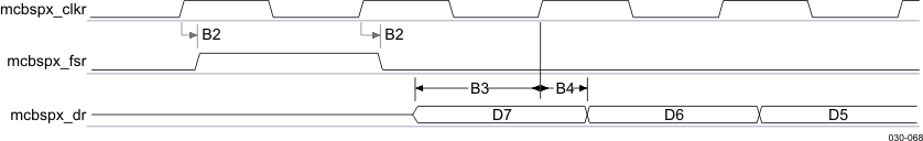 Figure 6-37 McBSP Rising Edge Receive Timing in Master Mode
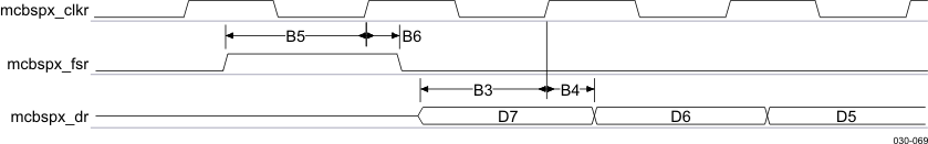 Figure 6-38 McBSP Rising Edge Receive Timing in Slave Mode
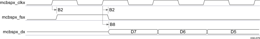 Figure 6-39 McBSP Rising Edge Transmit Timing in Master Mode
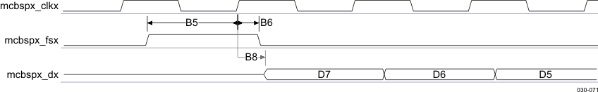 Figure 6-40 McBSP Rising Edge Transmit Timing in Slave Mode
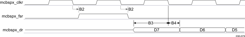 Figure 6-41 McBSP Falling Edge Receive Timing in Master Mode
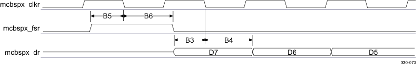 Figure 6-42 McBSP Falling Edge Receive Timing in Slave Mode
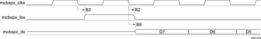 Figure 6-43 McBSP Falling Edge Transmit Timing in Master Mode
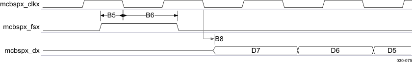 Figure 6-44 McBSP Falling Edge Transmit Timing in Slave Mode
6.6.2 Multichannel Serial Port Interface (McSPI) Timing
The multichannel SPI is a master/slave synchronous serial bus. The McSPI1 module supports up to four peripherals and the others (McSPI2, McSPI3, and McSPI4) support up to two peripherals. The following timings are applicable to the different configurations of McSPI in master/slave mode for any McSPI and any channel (n).
6.6.2.1 McSPI in Slave Mode
Table 6-92 and Table 6-93 assume testing over the recommended operating conditions.
Table 6-92 McSPI Interface Timing Requirements – Slave Mode
| NO. | PARAMETER | 1.8 V | 3.3 V | UNIT | |||
|---|---|---|---|---|---|---|---|
| MIN | MAX | MIN | MAX | ||||
| SS0 | tc(CLK) | Cycle time, mcspix_clk | 41.67 | 41.67 | ns | ||
| SS1 | tw(CLK) | Pulse duration, mcspix_clk high or low | 18.75 | 22.92 | 11.25 | ns | |
| SS2 | tsu(SIMOV-CLKAE) | Setup time, mcspix_simo valid before mcspix_clk active edge | 4.2 | 4 | ns | ||
| SS3 | th(SIMOV-CLKAE) | Hold time, mcspix_simo valid after mcspix_clk active edge | 4.6 | 3 | ns | ||
| SS4 | tsu(CS0V-CLKFE) | Setup time, mcspix_cs0 valid before mcspix_clk first edge | 13.8 | 7 | ns | ||
| SS5 | th(CS0I-CLKLE) | Hold time, mcspix_cs0 invalid after mcspix_clk last edge | 13.8 | 9.17 | ns | ||
Table 6-93 McSPI Interface Switching Characteristics(1)(2)(3)(4)
| NO. | PARAMETER | 1.8 V | 3.3 V | UNIT | ||||
|---|---|---|---|---|---|---|---|---|
| MIN | MAX | MIN | MAX | |||||
| SS6 | td(CLKAE-SOMIV) | Delay time, mcspix_clk active edge to mcspix_somi shifted | 1.8 | 15.9 | 2 | 16.5 | ns | |
| SS7 | td(CS0AE-SOMIV) | Delay time, mcspix_cs0 active edge to mcspix_somi shifted | Modes 0 and 2 | 16.38 | 15.9 | ns | ||
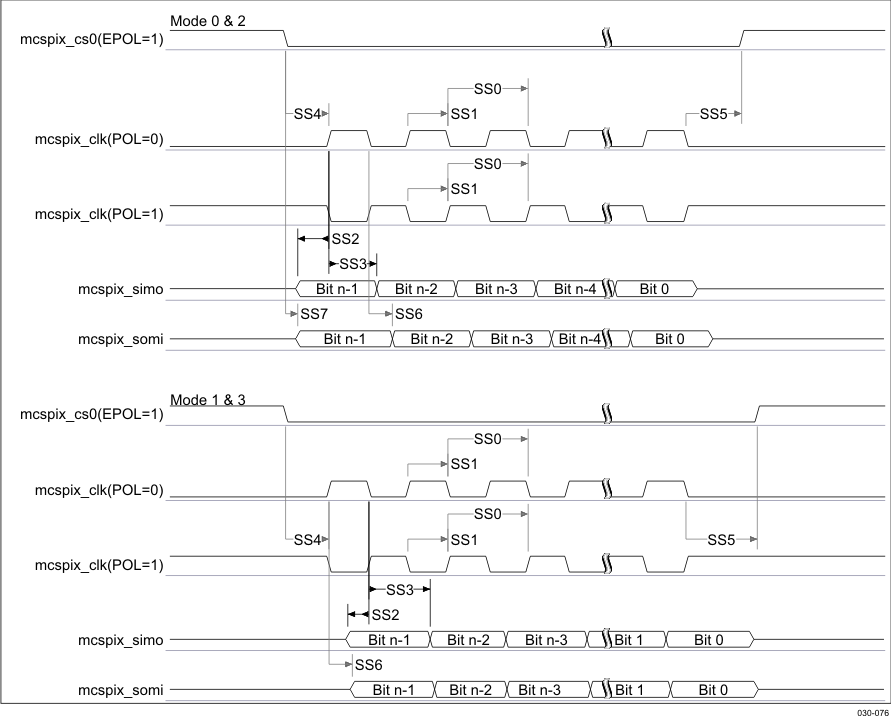
- The active clock edge (rising or falling) on which mcspi_somi is driven and mcspi_simo data is latched is software configurable with the bit MSPI_CHCONFx[0] = PHA and the bit MSPI_CHCONFx[1] = POL.
- The polarity of mcspix_csi is software configurable with the bit MSPI_CHCONFx[6] = EPOL In mcspix, x is equal to 1, 2, 3, or 4.
6.6.2.2 McSPI in Master Mode
Table 6-94 and Table 6-95 assume testing over the recommended operating conditions.
Table 6-94 McSPI1, 2, and 4 Interface Timing Requirements – Master Mode(1)(2)
| NO. | PARAMETER | 1.8 V | 3.3 V | UNIT | |||
|---|---|---|---|---|---|---|---|
| MIN | MAX | MIN | MAX | ||||
| SM2 | tsu(SOMIV-CLKAE) | Setup time, mcspix_somi valid before mcspix_clk active edge | 2.56 | 4 | ns | ||
| SM3 | th(SOMIV-CLKAE) | Hold time, mcspix_somi valid after mcspix_clk active edge | 2.93 | 4 | ns | ||
Table 6-95 McSPI1, 2, and 4 Interface Switching Characteristics – Master Mode(1)(3)(4)
| NO. | PARAMETER | 1.8 V | 3.3 V | UNIT | ||||
|---|---|---|---|---|---|---|---|---|
| MIN | MAX | MIN | MAX | |||||
| SM0 | tc(CLK) | Cycle time, mcspix_clk | 20.83 | 20.83 | ns | |||
| tj(CLK) | Cycle jitter(7), mcspix_clk | -200 | 200 | -200 | 200 | ps | ||
| SM1 | tw(CLK) | Pulse duration, mcspix_clk high or low | 0.45P(2) | 0.55P(2) | 0.45P(2) | 0.55P(2) | ns | |
| SM4 | td(CLKAE-SIMOV) | Delay time, mcspix_clk active edge to mcspix_simo shifted | -2.1 | 5 | -3 | 6 | ns | |
| SM5 | td(CSnA-CLKFE) | Delay time, mcspix_csi active to mcspix_clk first edge | Modes 1 and 3 | A(5) - 3.2 | A(5) - 3.0 | 6 | ns | |
| Modes 0 and 2 | B(6) - 3.2 | B(6) -3.0 | 6 | ns | ||||
| SM6 | td(CLKLE-CSnI) | Delay time, mcspix_clk last edge to mcspix_csi inactive | Modes 1 and 3 | B(6) - 3.2 | B(6) - 3.0 | ns | ||
| Modes 0 and 2 | A(5) - 3.2 | A(5) - 3.0 | ns | |||||
| SM7 | td(CSnAE-SIMOV) | Delay time, mcspix_csi active edge to mcspix_simo shifted | Modes 0 and 2 | 5 | 5 | ns | ||
Table 6-96 and Table 6-97 assume testing over the recommended operating conditions.
Table 6-96 McSPI 3 Interface Timing Requirements – Master Mode(1)(2)
| NO. | PARAMETER | 1.8 V | 3.3 V | UNIT | |||
|---|---|---|---|---|---|---|---|
| MIN | MAX | MIN | MAX | ||||
| SM2 | tsu(SOMIV-CLKAE) | Setup time, mcspi3_somi valid before mcspi3_clk active edge | 2.5 | 4 | ns | ||
| SM3 | th(SOMIV-CLKAE) | Hold time, mcspi3_somi valid after mcspi3_clk active edge | 2.89 | 4 | ns | ||
Table 6-97 McSPI3 Interface Switching Characteristics – Master Mode(1)(2)(3)
| NO. | PARAMETER | 1.8 V | 3.3 V | UNIT | ||||
|---|---|---|---|---|---|---|---|---|
| MIN | MAX | MIN | MAX | |||||
| SM0 | tc(CLK) | Cycle time, mcspix_clk | 41.67 | 41.67 | ns | |||
| tj(CLK) | Cycle jitter(6) | -200 | 200 | -200 | 200 | ps | ||
| SM1 | tw(CLK) | Pulse duration, mcspix_clk high or low | 0.45P(7) | 0.55P(7) | 0.45P(7) | 0.55P(7) | ns | |
| SM4 | td(CLKAE-SIMOV) | Delay time, mcspix_clk active edge to mcspix_simo shifted | -2.1 | 11.3 | -3 | ns | ||
| SM5 | td(CSnA-CLKFE) | Delay time, mcspix_csi active to mcspix_clk first edge | Modes 1 and 3 | A(4) - 4.4 | A(4) - 3.0 | 6 | ns | |
| Modes 0 and 2 | B(5) - 4.4 | B(5) - 3.0 | 6 | ns | ||||
| SM6 | td(CLKLE-CSnI) | Delay time, mcspix_clk last edge to mcspix_csi inactive | Modes 1 and 3 | B(5) - 4.4 | B(5) - 3.0 | ns | ||
| Modes 0 and 2 | A(4) - 4.4 | A(4) - 3.0 | ns | |||||
| SM7 | td(CSnAE-SIMOV) | Delay time, mcspix_csi active edge to mcspix_simo shifted | Modes 0 and 2 | 11.3 | 5 | ns | ||
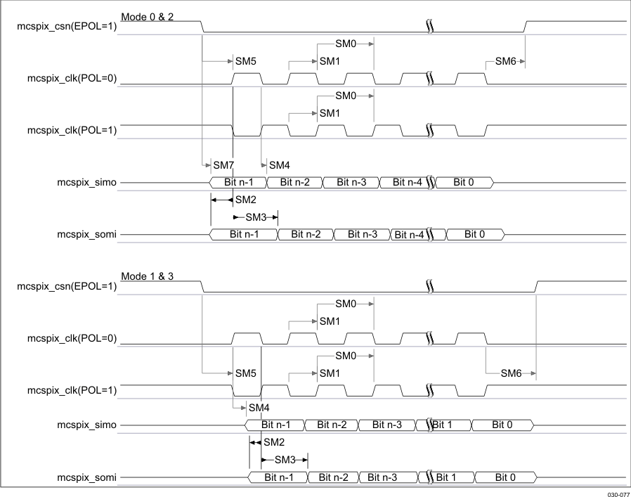
- The active clock edge (rising or falling) on which mcspix_simo is driven and mcspi_somi data is latched is software configurable with the bit MSPI_CHCONFx[0] = PHA and the bit MSPI_CHCONFx[1] = POL.
- The polarity of mcspix_csi is software configurable with the bit MSPI_CHCONFx[6] = EPOL.
- In mcspix, x is equal to 1. In mcspix_csn, n is equal to 0, 1, 2, or 3.
6.6.3 Multiport Full-Speed Universal Serial Bus (USB) Interface
The AM3517/05 microprocessor provides three USB ports working in full- and low-speed data transactions (up to 12Mbit/s).
Connected to either a serial link controller or a serial PHY (PHY interface modes) it supports:
- 6-pin (Tx: Dat/Se0 or Tx: Dp/Dm) unidirectional mode
- 4-pin bidirectional mode
- 3-pin bidirectional mode
6.6.3.1 Multiport Full-Speed Universal Serial Bus (USB) – Unidirectional Standard 6-pin Mode
Table 6-98 through Table 6-100 assume testing over the recommended operating conditions.
Table 6-98 Low-/Full-Speed USB Timing Conditions Unidirectional Standard 6-pin Mode
| TIMING CONDITION PARAMETER | 1.8V, 3.3V | UNIT | |
|---|---|---|---|
| Input Conditions | |||
| tR | Input signal rise time | 2.0 | ns |
| tF | Input signal fall time | 2.0 | ns |
| Output Conditions | |||
| CLOAD | Output load capacitance | 15.0 | pF |
Table 6-99 Low-/Full-Speed USB Timing Requirements Unidirectional Standard 6-pin Mode
| NO. | PARAMETER | 1.8V, 3.3V | UNIT | ||
|---|---|---|---|---|---|
| MIN | MAX | ||||
| FSU1 | td(Vp,Vm) | Time duration, mmx_rxdp and mmx_rxdm low together during transition | 14.0 | ns | |
| FSU2 | td(Vp,Vm) | Time duration, mmx_rxdp and mmx_rxdm high together during transition | 8.0 | ns | |
| FSU3 | td(RCVU0) | Time duration, mmx_rrxcv undefine during a single end 0 (mmx_rxdp and mmx_rxdm low together) | 14.0 | ns | |
| FSU4 | td(RCVU1) | Time duration, mmx_rxrcv undefine during a single end 1 (mmx_rxdp and mmx_rxdm high together) | 8.0 | ns | |
Table 6-100 Low-/Full-Speed USB Switching Characteristics Unidirectional Standard 6-pin Mode
| NO. | PARAMETER | 1.8V, 3.3V | UNIT | ||
|---|---|---|---|---|---|
| MIN | MAX | ||||
| FSU5 | td(TXENL-DATV) | Delay time, mmx_txen_n low to mmx_txdat valid | 81.8 | 84.8 | ns |
| FSU6 | td(TXENL-SE0V) | Delay time, mmx_txen_n low to mmx_txse0 valid | 81.8 | 84.8 | ns |
| FSU7 | ts(DAT-SE0) | Skew between mmx_txdat and mmx_txse0 transition | 1.5 | ns | |
| FSU8 | td(DATI-TXENH) | Delay time, mmx_txdat invalid to mmx_txen_n high | 81.8 | ns | |
| FSU9 | td(SE0I-TXENH) | Delay time, mmx_txse0 invalid to mmx_txen_n high | 81.8 | ns | |
| tR(do) | Rise time, mmx_txen_n | 4.0 | ns | ||
| tF(do) | Fall time, mmx_txen_n | 4.0 | ns | ||
| tR(do) | Rise time, mmx_txdat | 4.0 | ns | ||
| tF(do) | Fall time, mmx_txdat | 4.0 | ns | ||
| tR(do) | Rise time, mmx_txse0 | 4.0 | ns | ||
| tF(do) | Fall time, mmx_txse0 | 4.0 | ns | ||
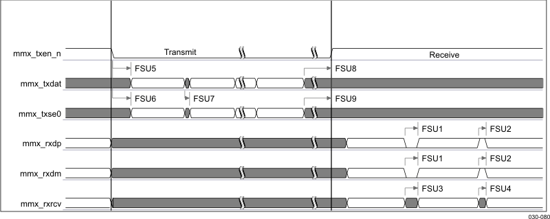
6.6.3.2 Multiport Full-Speed Universal Serial Bus (USB) – Bidirectional Standard 4-pin Mode
Table 6-101 through Table 6-103 assume testing over the recommended operating conditions.
Table 6-101 Low-/Full-Speed USB Timing Conditions Bidirectional Standard 4-pin Mode
| TIMING CONDITION PARAMETER | 1.8V, 3.3V | UNIT | |
|---|---|---|---|
| Input Conditions | |||
| tR | Input signal rise time | 2.0 | ns |
| tF | Input signal fall time | 2.0 | ns |
| Output Conditions | |||
| CLOAD | Output load capacitance | 15.0 | pF |
Table 6-102 Low-/Full-Speed USB Timing Requirements Bidirectional Standard 4-pin Mode
| NO. | PARAMETER | 1.8V, 3.3V | UNIT | ||
|---|---|---|---|---|---|
| MIN | MAX | ||||
| FSU10 | td(DAT,SE0) | Time duration, mmx_txdat and mmx_txse0 low together during transition | 14.0 | ns | |
| FSU11 | td(DAT,SE0) | Time duration, mmx_txdat and mmx_txse0 high together during transition | 8.0 | ns | |
| FSU12 | td(RCVU0) | Time duration, mmx_rrxcv undefine during a single end 0 (mmx_txdat and mmx_txse0 low together) | 14.0 | ns | |
| FSU13 | td(RCVU1) | Time duration, mmx_rxrcv undefine during a single end 1 (mmx_txdat and mmx_txse0 high together) | 8.0 | ns | |
Table 6-103 Low-/Full-Speed USB Switching Characteristics Bidirectional Standard 4-pin Mode
| NO. | PARAMETER | 1.8V, 3.3V | UNIT | ||
|---|---|---|---|---|---|
| MIN | MAX | ||||
| FSU14 | td(TXENL-DATV) | Delay time, mmx_txen_n low to mmx_txdat valid | 81.8 | 84.8 | ns |
| FSU15 | td(TXENL-SE0V) | Delay time, mmx_txen_n low to mmx_txse0 valid | 81.8 | 84.8 | ns |
| FSU16 | ts(DAT-SE0) | Skew between mmx_txdat and mmx_txse0 transition | 1.5 | ns | |
| FSU17 | td(DATV-TXENH) | Delay time, mmx_txdat invalid before mmx_txen_n high | 81.8 | ns | |
| FSU18 | td(SE0V-TXENH) | Delay time, mmx_txse0 invalid before mmx_txen_n high | 81.8 | ns | |
| tR(txen) | Rise time, mmx_txen_n | 4.0 | ns | ||
| tF(txen) | Fall time, mmx_txen_n | 4.0 | ns | ||
| tR(dat) | Rise time, mmx_txdat | 4.0 | ns | ||
| tF(dat) | Fall time, mmx_txdat | 4.0 | ns | ||
| tR(se0) | Rise time, mmx_txse0 | 4.0 | ns | ||
| tF(se0) | Fall time, mmx_txse0 | 4.0 | ns | ||
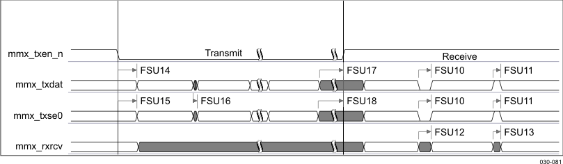
6.6.3.3 Multiport Full-Speed Universal Serial Bus (USB) – Bidirectional Standard 3-pin Mode
Table 6-104 through Table 6-106 assume testing over the recommended operating conditions.
Table 6-104 Low-/Full-Speed USB Timing Conditions Bidirectional Standard 3-pin Mode
| TIMING CONDITION PARAMETER | 1.8V, 3.3V | UNIT | |
|---|---|---|---|
| Input Conditions | |||
| tR | Input signal rise time | 2.0 | ns |
| tF | Input signal fall time | 2.0 | ns |
| Output Conditions | |||
| CLOAD | Output load capacitance | 15.0 | pF |
Table 6-105 Low-/Full-Speed USB Timing Requirements Bidirectional Standard 3-pin Mode
| NO. | PARAMETER | 1.8V, 3.3V | UNIT | ||
|---|---|---|---|---|---|
| MIN | MAX | ||||
| FSU19 | td(DAT,SE0) | Time duration, mmx_txdat and mmx_txse0 low together during transition | 14.0 | ns | |
| FSU20 | td(DAT,SE0) | Time duration, mmx_tsdat and mmx_txse0 high together during transition | 8.0 | ns | |
Table 6-106 Low-/Full-Speed USB Switching Characteristics Bidirectional Standard 3-pin Mode
| NO. | PARAMETER | 1.8V, 3.3V | UNIT | ||
|---|---|---|---|---|---|
| MIN | MAX | ||||
| FSU21 | td(TXENL-DATV) | Delay time, mmx_txen_n low to mmx_txdat valid | 81.8 | 84.8 | ns |
| FSU22 | td(TXENL-SE0V) | Delay time, mmx_txen_n low to mmx_txse0 valid | 81.8 | 84.8 | ns |
| FSU23 | ts(DAT-SE0) | Skew between mmx_txdat and mmx_txse0 transition | 1.5 | ns | |
| FSU24 | td(DATI-TXENH) | Delay time, mmx_txdat invalid to mmx_txen_n high | 81.8 | ns | |
| FSU25 | td(SE0I-TXENH) | Delay time, mmx_txse0 invalid to mmx_txen_n high | 81.8 | ns | |
| tR(do) | Rise time, mmx_txen_n | 4.0 | ns | ||
| tF(do) | Fall time, mmx_txen_n | 4.0 | ns | ||
| tR(do) | Rise time, mmx_txdat | 4.0 | ns | ||
| tF(do) | Fall time, mmx_txdat | 4.0 | ns | ||
| tR(do) | Rise time, mmx_txse0 | 4.0 | ns | ||
| tF(do) | Fall time, mmx_txse0 | 4.0 | ns | ||
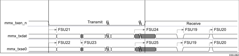
6.6.4 Multiport High-Speed Universal Serial Bus (USB) Timing
In addition to the full-speed USB controller, a high-speed (HS) USB controller is instantiated inside the AM3517/05. It allows high-speed transactions (up to 480 Mbit/s) on the USB ports 1 and 2.
- Port 1 and port 2:
- 12-bit master mode (SDR)
6.6.4.1 High-Speed Universal Serial Bus (USB) on Ports 1 and 2 12-bit Master Mode
Table 6-107 through Table 6-109 assume testing over the recommended operating conditions.
Table 6-107 High-Speed USB Timing Conditions 12-bit Master Mode
| TIMING CONDITION PARAMETER | 1.8V, 3.3V | UNIT | |
|---|---|---|---|
| Input Conditions | |||
| tR | Input signal rise time | 2 | ns |
| tF | Input signal fall time | 2 | ns |
| Output Conditions | |||
| CLOAD | Output load capacitance | 3 | pF |
Table 6-108 High-Speed USB Timing Requirements 12-bit Master Mode(1)
| NO. | PARAMETER | 1.8V, 3.3V | UNIT | ||
|---|---|---|---|---|---|
| MIN | MAX | ||||
| HSU3 | ts(DIRV-CLKH) | Setup time, hsusbx_dir valid before hsusbx_clk rising edge | 7.5 | ns | |
| ts(NXTV-CLKH) | Setup time, hsusbx_nxt valid before hsusbx_clk rising edge | 7.5 | ns | ||
| HSU4 | th(CLKH-DIRIV) | Hold time, hsusbx_dir valid after hsusbx_clk rising edge | 0.2 | ns | |
| th(CLKH-NXT/IV) | Hold time, hsusbx_nxt valid after hsusbx_clk rising edge | 0.2 | ns | ||
| HSU5 | ts(DATAV-CLKH) | Setup time, hsusbx_data[0:7] valid before hsusbx_clk rising edge | 7.5 | ns | |
| HSU6 | th(CLKH-DATIV) | Hold time, hsusbx_data[0:7] valid after hsusbx_clk rising edge | 0.2 | ns | |
Table 6-109 High-Speed USB Switching Characteristics 12-bit Master Mode(1)
| N O. | PARAMETER | 1.8V, 3.3V | UNIT | ||
|---|---|---|---|---|---|
| MIN | MAX | ||||
| HSU0 | fp(CLK) | hsusbx_clk clock frequency | 60 | MHz | |
| tj(CLK) | Jitter standard deviation(2), hsusbx_clk | 200 | ps | ||
| HSU1 | td(CLKH-STPV) | Delay time, hsusbx_clk high to output hsusbx_stp valid | 13 | ns | |
| td(CLKH-STPIV) | Delay time, hsusbx_clk high to output hsusbx_stp invalid | 2 | ns | ||
| HSU2 | td(CLKH-DV) | Delay time, hsusbx_clk high to output hsusbx_data[0:7] valid | 13 | ns | |
| td(CLKH-DIV) | Delay time, hsusbx_clk high to output hsusbx_data[0:7] invalid | 2 | ns | ||
| tR(do) | Rise time, output signals | 2 | ns | ||
| tF(do) | Fall time, output signals | 2 | ns | ||
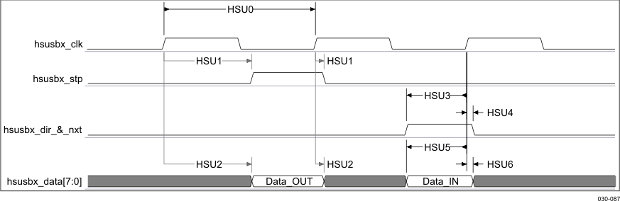
6.6.5 USB0 OTG (USB2.0 OTG)
The AM3517/05 USB2.0 peripheral supports the following features:
- USB 2.0 peripheral at speeds high speed (HS: 480 Mb/s) and full speed (FS: 12 Mb/s)
- USB 2.0 host at speeds HS, FS, and low speed (LS: 1.5 Mb/s)
- All transfer modes (control, bulk, interrupt, and isochronous)
- 16 Transmit (TX) and 16 Receive (RX) endpoints in addition to endpoint 0
- FIFO RAM
- 32K endpoint
- Programmable size
- Integrated USB 2.0 High Speed PHY
- Connects to a standard Charge Pump for VBUS 5 V generation
- RNDIS mode for accelerating RNDIS type protocols using short packet termination over USB
6.6.5.1 USB OTG Electrical Parameters
The USB OTG electrical parameters meet or exceed those specified in the following documents which can be obtained from the USB Implementers Forum:
- Universal Serial Bus Specification, Revision 2.0, April 27, 2000
- On-The-Go Supplement to the USB 2.0 Specification, Revision 1.3, December 5, 2006
- Engineering Change Notice “Pull-up/pull-down resistors”, Universal Serial Bus Specification Revision 2.0
For additional information related to USB OTG electrical parameters, please see the respective documents on the USB Implementers Forum web site (http://www.usb.org).
6.6.6 High-End Controller Area Network Controller (HECC) Timing
The AM3517/05 device has a High-End Controller Area Network Controller (HECC). The HECC uses established protocol to communicate serially with other controllers in harsh environments. The HECC is fully compliant with the Controller Area Network (CAN) protocol, version 2.0B.
Key features of the HECC include the following:
- CAN, version 2.0B compliant
- 32 RX/TX message objects
- 32 receive identifier masks
- Programmable wake-up on bus activity
- Programmable interrupt scheme
- Automatic reply to a remote request
- Automatic re-transmission in case of error or loss of arbitration
- Protection against reception of a new message
- 32-bit time stamp
- Local network time counter
- Programmable priority register for each message
- Programmable transmission and reception time-out
- HECC/SCC mode of operation
- Standard-Extended Identifier
- Self-test mode
6.6.6.1 HECC Timing Requirements
Table 6-110 Timing Requirements for HECC Receive (see Figure 6-51)
| NO. | 1.8 V, 3.3 V | UNIT | |||
|---|---|---|---|---|---|
| MIN | MAX | ||||
| 1 | f(baud) | Maximum programmable baud rate | 1 | Mbps | |
| 2 | tw(HECC_RX) | Pulse duration, receive data bit | H-1(1) | H+3(1) | ns |
6.6.6.2 HECC Switching Characteristics
Table 6-111 Switching Characteristics Over Recommended Operating Conditions for HECC Transmit
(see Figure 6-51)
| NO. | PARAMETER | 1.8 V, 3.3 V | UNIT | ||
|---|---|---|---|---|---|
| MIN | MAX | ||||
| 3 | f(baud) | Maximum programmable baud rate | 1 | Mbps | |
| 4 | tw(HECC_TX) | Pulse duration, transmit data bit | H-1(1) | H+3(1) | ns |
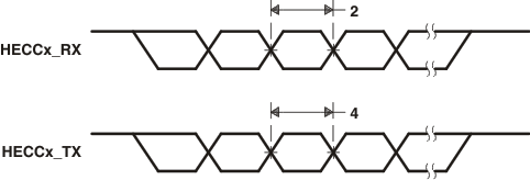 Figure 6-51 HECC Transmit/Receive Timing
6.6.7 Ethernet Media Access Controller (EMAC)
The Ethernet Media Access Controller (EMAC) provides an efficient interface between the AM3517/05 and the network. The EMAC supports both 10Base-T and 100Base-TX, or 10 Mbits/second (Mbps) and 100 Mbps in either half- or full-duplex mode, with hardware flow control and quality of service (QOS) support.
The EMAC controls the flow of packet data from the AM3517/05 device to the PHY. The MDIO module controls PHY configuration and status monitoring.
Both the EMAC and the MDIO modules interface to the AM3517/05 device through a custom interface that allows efficient data transmission and reception. This custom interface is referred to as the EMAC control module, and is considered integral to the EMAC/MDIO peripheral. The control module is also used to multiplex and control interrupts.
6.6.7.1 EMAC Electrical Data/ Timing
Table 6-112 through Table 6-114 assume testing over the recommended operating conditions.
Table 6-112 RMII Input Timing Requirements
| NO. | PARAMETER | 1.8V, 3.3V | ||||
|---|---|---|---|---|---|---|
| MIN | TYP | MAX | UNIT | |||
| fc(REFCLK) | Frequency, REF_CLK | 50 | MHz | |||
| ft (REFCLK) | Frequency stability, REF_CLK | +/-50 | ppm | |||
| 1 | tc(REFCLK) | Cycle Time, REF_CLK | 20 | ns | ||
| 2 | tw(REFCLKH) | Pulse Width, REF_CLK High | 7 | 13 | ns | |
| 3 | tw(REFCLKL) | Pulse Width, REF_CLK Low | 7 | 13 | ns | |
| 6 | tsu(RXD-REFCLK) | Input Setup Time, RXD Valid before REF_CLK High | 4 | ns | ||
| 7 | th(REFCLK-RXD) | Input Hold Time, RXD Valid after REF_CLK High | 2 | ns | ||
| 8 | tsu(CRSDV-REFCLK) | Input Setup Time, CRSDV Valid before REF_CLK High | 4 | ns | ||
| 9 | th(REFCLK-CRSDV) | Input Hold Time, CRSDV Valid after REF_CLK High | 2 | ns | ||
| 10 | tsu(RXER-REFCLK) | Input Setup Time, RXER Valid before REF_CLK High | 4 | ns | ||
| 11 | th(REFCLKR-RXER) | Input Hold Time, RXER Valid after REF_CLK High | 2 | ns | ||
Table 6-113 RMII Timing Conditions
| TIMING CONDITION PARAMETER | 1.8V, 3.3V | UNIT | ||
|---|---|---|---|---|
| Input Conditions | MIN | MAX | ||
| tR | Input signal rise time | 1 | 5 | ns |
| tF | Input signal fall time | 1 | 5 | ns |
| Output Conditions | ||||
| CLOAD | Output load capacitance | 5.5 | pF | |
Table 6-114 RMII Output Switching Characteristics
| NO. | PARAMETER | 1.8V, 3.3V | ||||
|---|---|---|---|---|---|---|
| MIN | TYP | MAX | UNIT | |||
| 4 | td(REFCLK-TXD) | Output Delay Time, REF_CLK High to TXD Valid | 2.5 | 13 | ns | |
| 5 | td(REFCLK-TXEN) | Output Delay Time, REF_CLK High to TXEN Valid | 2.5 | 13 | ns | |
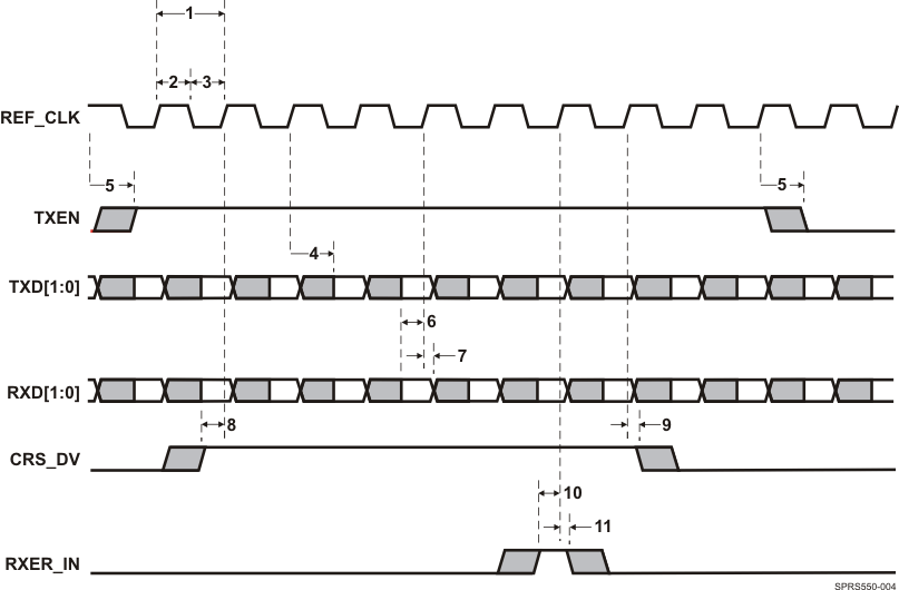 Figure 6-52 RMII Timing Diagram
6.6.8 Management Data Input/Output (MDIO)
The Management Data Input/Output (MDIO) module continuously polls all 32 MDIO addresses in order to enumerate all PHY devices in the system.
The Management Data Input/Output (MDIO) module implements the 802.3 serial management interface to interrogate and control Ethernet PHY(s) using a shared two-wire bus. Host software uses the MDIO module to configure the auto-negotiation parameters of each PHY attached to the EMAC, retrieve the negotiation results, and configure required parameters in the EMAC module for correct operation. The module is designed to allow almost transparent operation of the MDIO interface, with very little maintenance from the core processor. Only one PHY may be connected at any given time.
6.6.8.1 Management Data Input/Output (MDIO) Electrical Data/Timing
Table 6-115 Timing Requirements for MDIO Input (see Figure 6-53 and Figure 6-54)
| No. | PARAMETER | UNIT | |||
|---|---|---|---|---|---|
| MIN | MAX | ||||
| 1 | tc(MD_CLK) | Cycle time, MD_CLK | 400 | ns | |
| 4 | tsu(MDIO-MDCLKH) | Setup time, MDIO data input valid before MD_CLK high | 20 | ns | |
| 5 | th(MDCLKH-MDIO) | Hold time, MDIO data input valid after MDCLK high | 0 | ns | |
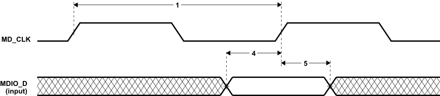 Figure 6-53 MDIO Input Timing
Table 6-116 Switching Characteristics Over Recommended Operating Conditions for MDIO Output
(see Figure 6-54)
| No. | PARAMETER | UNIT | |||
|---|---|---|---|---|---|
| MIN | MAX | ||||
| 7 | td(MDCLKL-MDIO) | Delay time, MDCLK low to MDIO data output valid | 0 | 100 | ns |
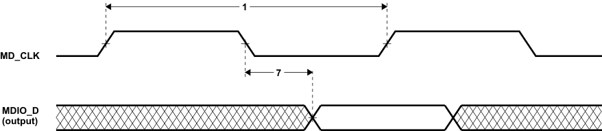 Figure 6-54 MDIO Output Timing
6.6.9 Universal Asynchronous Receiver/Transmitter (UART)
The AM3517/05 has four UARTs (one with Infrared Data Association [IrDA] and Consumer Infrared [CIR] modes).
Table 6-117 Timing Requirements for UARTx Receive(1)
| NO. | 1.8V, 3.3V | UNIT | |||
|---|---|---|---|---|---|
| MIN | MAX | ||||
| 4 | tw(URXDB) | Pulse duration, receive data bit (RXDn) | .96U | 1.05U | ns |
| 5 | tw(URXSB) | Pulse duration, receive start bit | .96U | 1.05U | ns |
Table 6-118 Switching Characteristics Over Recommended Operating Conditions for UARTx Transmit(1)
| NO. | PARAMETER | 1.8V, 3.3V | UNIT | ||
|---|---|---|---|---|---|
| MIN | MAX | ||||
| 1 | f(baud) | UART0 Maximum programmable baud rate f(baud_15) | 5 | mbps | |
| UART0 Maximum programmable baud rate f(baud_30) | 0.23 | ||||
| UART0 Maximum programmable baud rate f(baud_100) | 0.115 | ||||
| 2 | tw(UTXDB) | Pulse duration, transmit data bit, 15/30/100 pF | U - 2 | U + 2 | ns |
| 3 | tw(UTXSB) | Pulse duration, transmit start bit, 15/30/100 pF | U - 2 | U + 2 | ns |
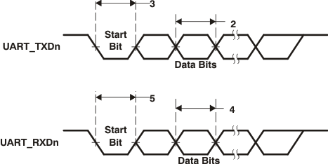 Figure 6-55 UART Transmit/Receive Timing
6.6.9.1 UART IrDA Interface
The IrDA module can operate in three different modes:
- Slow infrared (SIR) (≤115.2 Kbits/s)
- Medium infrared (MIR) (0.576 Mbits/s and 1.152 Mbits/s)
- Fast infrared (FIR) (4 Mbits/s)
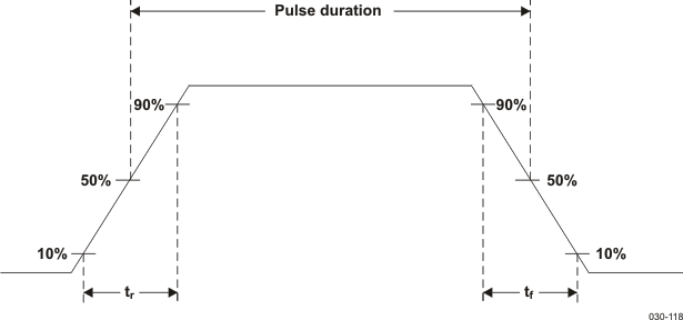 Figure 6-56 UART IrDA Pulse Parameters
6.6.9.1.1 IrDA—Receive Mode
Table 6-119 UART IrDA—Signaling Rate and Pulse Duration—Receive Mode
| SIGNALING RATE | ELECTRICAL PULSE DURATION | UNIT | ||
|---|---|---|---|---|
| MIN | NOMINAL | MAX | ||
| SIR | ||||
| 2.4 Kbit/s | 1.41 | 78.1 | 88.55 | μs |
| 9.6 Kbit/s | 1.41 | 19.5 | 22.13 | μs |
| 19.2 Kbit/s | 1.41 | 9.75 | 11.07 | μs |
| 38.4 Kbit/s | 1.41 | 4.87 | 5.96 | μs |
| 57.6 Kbit/s | 1.41 | 3.25 | 4.34 | μs |
| 115.2 Kbit/s | 1.41 | 1.62 | 2.23 | μs |
| MIR | ||||
| 0.576 Mbit/s | 297.2 | 416 | 518.8 | ns |
| 1.152 Mbit/s | 149.6 | 208 | 258.4 | ns |
| FIR | ||||
| 4.0 Mbit/s (Single pulse) | 67 | 125 | 164 | ns |
| 4.0 Mbit/s (Double pulse) | 190 | 250 | 289 | ns |
Table 6-120 UART IrDA—Rise and Fall Time—Receive Mode
| PARAMETER | MAX | UNIT | |
|---|---|---|---|
| tR | Rising time, uart3_rx_irrx | 200 | ns |
| tF | Falling time, uart3_rx_irrx | 200 | ns |
6.6.9.1.2 IrDA—Transmit Mode
Table 6-121 UART IrDA—Signaling Rate and Pulse Duration—Transmit Mode
| SIGNALING RATE | ELECTRICAL PULSE DURATION | UNIT | ||
|---|---|---|---|---|
| MIN | NOMINAL | MAX | ||
| SIR | ||||
| 2.4 Kbit/s | 78.1 | 78.1 | 78.1 | μs |
| 9.6 Kbit/s | 19.5 | 19.5 | 19.5 | μs |
| 19.2 Kbit/s | 9.75 | 9.75 | 9.75 | μs |
| 38.4 Kbit/s | 4.87 | 4.87 | 4.87 | μs |
| 57.6 Kbit/s | 3.25 | 3.25 | 3.25 | μs |
| 115.2 Kbit/s | 1.62 | 1.62 | 1.62 | μs |
| MIR | ||||
| 0.576 Mbit/s | 414 | 416 | 419 | ns |
| 1.152 Mbit/s | 206 | 208 | 211 | ns |
| FIR | ||||
| 4.0 Mbit/s (Single pulse) | 123 | 125 | 128 | ns |
| 4.0 Mbit/s (Double pulse) | 248 | 250 | 253 | ns |
6.6.10 HDQ / 1-Wire Interfaces
This module is intended to work with both the HDQ and the 1-Wire protocols. The protocols use a single wire to communicate between the master and the slave. The protocols employ an asynchronous return to 1 mechanism where, after any command, the line is pulled high.
6.6.10.1 HDQ Protocol
Table 6-122 and Table 6-123 assume testing over the recommended operating conditions (see Figure 6-57 through Figure 6-60).
Table 6-122 HDQ Timing Requirements
| PARAMETER | DESCRIPTION | MIN | MAX | UNIT |
|---|---|---|---|---|
| tCYCD | Bit window | 253 | s | |
| tHW1 | Reads 1 | 68 | ||
| tHW0 | Reads 0 | 180 | ||
| tRSPS | Command to host respond time(1) |
Table 6-123 HDQ Switching Characteristics
| PARAMETER | DESCRIPTION | MIN | TYP | MAX | UNIT |
|---|---|---|---|---|---|
| tB | Break timing | 193 | s | ||
| tBR | Break recovery | 63 | |||
| tCYCH | Bit window | 253 | |||
| tDW1 | Sends1 (write) | 1.3 | |||
| tDW0 | Sends0 (write) | 101 |
 Figure 6-57 HDQ Break (Reset) Timing
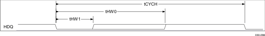 Figure 6-58 HDQ Read Bit Timing (Data)
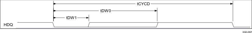 Figure 6-59 HDQ Write Bit Timing (Command/Address or Data)
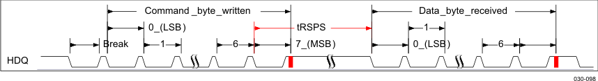 Figure 6-60 HDQ Communication Timing
6.6.10.2 1-Wire Protocol
Table 6-124 and Table 6-125 assume testing over the recommended operating conditions (see Figure 6-61 through Figure 6-63).
Table 6-124 1-Wire Timing Requirements
| PARAMETER | DESCRIPTION | MIN | MAX | UNIT |
|---|---|---|---|---|
| tPDH | Presence pulse delay high | 68 | s | |
| tPDL | Presence pulse delay low | 68 tPDH | ||
| tRDV + tREL | Read bit-zero time | 102 |
Table 6-125 1-Wire Switching Characteristics
| PARAMETER | DESCRIPTION | MIN | TYP | MAX | UNIT |
|---|---|---|---|---|---|
| tRSTL | Reset time low | 484 | s | ||
| tRSTH | Reset time high | 484 | |||
| tSLOT | Write bit cycle time | 102 | |||
| tLOW1 | Write bit-one time | 1.3 | |||
| tLOW0 | Write bit-zero time | 101 | |||
| tREC | Recovery time | 134 | |||
| tLOWR | Read bit strobe time | 13 |
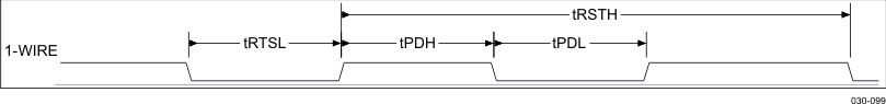 Figure 6-61 1-Wire Break (Reset) Timing
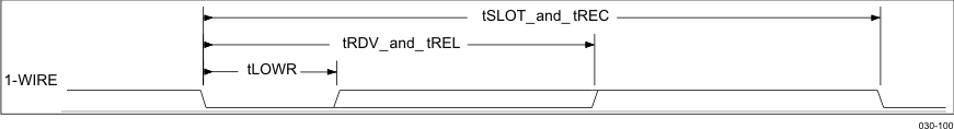 Figure 6-62 1-Wire Read Bit Timing (Data)
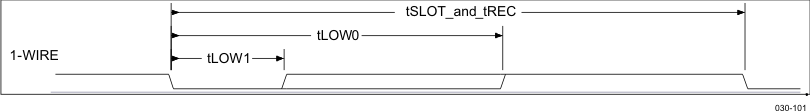 Figure 6-63 1-Wire Write Bit Timing (Command/Address or Data)
6.6.11 I2C Interface
The multimaster I2C peripheral provides an interface between two or more devices via an I2C serial bus. The I2C controller supports the multimaster mode which allows more than one device capable of controlling the bus to be connected to it. Each I2C device is recognized by a unique address and can operate as either transmitter or receiver, according to the function of the device. In addition to being a transmitter or receiver, a device connected to the I2C bus can also be considered as master or slave when performing data transfers. This data transfer is carried out via two serial bidirectional wires:
- An SDA data line
- An SCL clock line
The following sections illustrate the data transfer is in master or slave configuration with 7-bit addressing format. The I2C interface is compliant with Philips I2C specification version 2.1. It supports standard mode (up to 100K bits/s), fast mode (up to 400K bits/s) and high-speed mode (up to 3.4Mb/s) .
6.6.11.1 I2C Standard/Fast-Speed Mode
Table 6-126 I2C Standard/Fast-Speed Mode Timings
| 1.8V, 3.3-V | |||||||
|---|---|---|---|---|---|---|---|
| NO. | PARAMETER(3) | STANDARD MODE | FAST MODE | UNIT | |||
| MIN | MAX | MIN | MAX | ||||
| fSCL | Clock Frequency, i2cX_scl | 100 | 400 | kHz | |||
| I1 | tw(SCLH) | Pulse Duration, i2cX_scl high | 4 | 0.6 | s | ||
| I2 | tw(SCLL) | Pulse Duration, i2cX_scl low | 4.7 | 1.3 | s | ||
| I3 | tsu(SDAV-SCLH) | Setup time, i2cX_sda valid before i2cX_scl active level | 250 | 100(1) | ns | ||
| I4 | th(SCLHSDAV) | Hold time, i2cX_sda valid after i2cX_scl active level | 3.45(2) | 0.9(2) | s | ||
| I5 | tsu(SDAL-SCLH) | Setup time, i2cX_scl high after i2cX_sda low (for a START(4) condition or a repeated START condition) | 4.7 | 0.6 | s | ||
| I6 | th(SCLHSDAH) | Hold time, i2cX_sda low level after i2cX_scl high level (STOP condition) | 4 | 0.6 | s | ||
| I7 | th(SCLHRSTART) | Hold time, i2cX_sda low level after i2cX_scl high level (for a repeated START condition) | 4 | 0.6 | s | ||
| I8 | tw(SDAH) | Pulse duration, i2cX_sda high between STOP and START conditions | 4.7 | 1.3 | s | ||
| tR(SCL) | Rise time, i2cX_scl | 1000 | 300 | ns | |||
| tF(SCL) | Fall time, i2cX_scl | 300 | 300 | ns | |||
| tR(SDA) | Rise time, i2cX_sda | 1000 | 300 | ns | |||
| tF(SDA) | Fall time, i2cX_sda | 300 | 300 | ns | |||
| CB | Capacitive load for each bus line | 60 | 60 | pF | |||
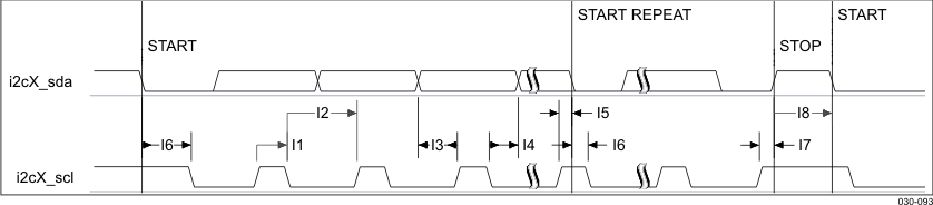 Figure 6-64 I2C Standard/Fast Mode
6.6.11.2 I2C High-Speed Mode
Table 6-127 I2C High-Speed Mode Timings(3)(4)
| 1.8V, 3.3V | |||||
|---|---|---|---|---|---|
| NO. | PARAMETER | UNIT | |||
| MIN | MAX | ||||
| fSCL | Clock frequency, i2cX_scl | 3.4 | MHz | ||
| I1 | tw(SCLH) | Pulse duration, i2cX_scl high | 60(1) | s | |
| I2 | tw(SCLL) | Pulse duration, i2cX_scl low | 160(1) | s | |
| I3 | tsu(SDAV-SCLH) | Setup time, i2cX_sda valid before i2cX_scl active level | 10 | ns | |
| I4 | th(SCLHSDAV) | Hold time, i2cX_sda valid after i2cX_scl active level | 70 | s | |
| I5 | tsu(SDAL-SCLH) | Setup time, i2cX_scl high after i2cX_sda low (for a START(2) condition or a repeated START condition) |
160 | s | |
| I6 | th(SCLHSDAH) | Hold time, i2cX_sda low level after i2cX_scl high level (STOP condition) | 160 | s | |
| I7 | th(SCLHRSTART) | Hold time, i2cX_sda low level after i2cX_scl high level (for a repeated START condition) | 160 | ns | |
| tR(SCL) | Rise time, i2cX_scl | 10 | 40 | ns | |
| tR(SCL) | Rise time, i2cX_scl after a repeated START condition and after a bit acknowledge | 10 | 80 | ns | |
| tF(SCL) | Fall time, i2cX_scl | 10 | 40 | ns | |
| tR(SDA) | Rise time, i2cX_sda | 10 | 80 | ns | |
| tF(SDA) | Fall time, i2cX_sda | 10 | 80 | ns | |
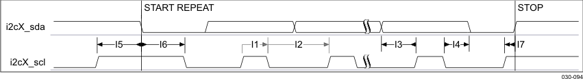
- HS-mode master devices generate a serial clock signal with a high-to-low ratio of 1 to 2. tw(SCLL) > 2 x tw(SCLH).
- In i2cX, X is equal to 1, 2, or 3.
- After this time, the first clock is generated.
Table 6-128 Correspondence Standard vs. TI Timing References
| AM3517/05 | STANDARD-I2C | ||
|---|---|---|---|
| S/F Mode | HS Mode | ||
| fSCL | FSCL | FSCLH | |
| I1 | tw(SCLH) | THIGH | THIGH |
| I2 | tw(SCLL) | TLOW | TLOW |
| I3 | tsu(SDAV-SCLH) | TSU;DAT | TSU;DAT |
| I4 | th(SCLH-SDAV) | TSU;DAT | TSU;DAT |
| I5 | tsu(SDAL-SCLH) | TSU;STA | TSU;STA |
| I6 | th(SCLH-SDAH) | THD;STA | THD;STA |
| I7 | th(SCLH-RSTART) | TSU;STO | TSU;STO |
| I8 | tw(SDAH) | TBUF | |
6.7 Removable Media Interfaces
6.7.1 High-Speed Multimedia Memory Card (MMC) and Secure Digital IO Card (SDIO) Timing
The MMC/SDIO host controller provides an interface to high-speed and standard MMC, SD memory cards, or SDIO cards. The application interface is responsible for managing transaction semantics. The MMC/SDIO host controller deals with MMC/SDIO protocol at transmission level, packing data, adding CRC, start/end bit, and checking for syntactical correctness.
There are three MMC interfaces on the AM3517/05:
- MMC/SD/SDIO Interface 1:
- 1.8-V/3.3-V support
- 8 bits
- MMC/SD/SDIO Interface 2:
- 1.8-V/3.3-V support
- 8 bits
- 4 bits with external transceiver allowing to support 1.8-V/3.3-V peripherals in 1.8-V mode operation. Transceiver direction control signals are multiplexed with the upper four data bits.
- MMC/SD/SDIO Interface 3:
- 1.8-V/3.3-V support
- 8 bits
6.7.1.1 MMC/SD/SDIO in SD Identification Mode
Table 6-129 through Table 6-131 assume testing over the recommended operating conditions and electrical characteristic conditions.
Table 6-129 MMC/SD/SDIO Timing Conditions SD Identification Mode
| TIMING CONDITION PARAMETER | 1.8V, 3.3V | UNIT | ||
|---|---|---|---|---|
| MIN | MAX | |||
| SD Identification Mode | ||||
| Input Conditions | ||||
| tr | Input signal rise time | 10 | ns | |
| tf | Input signal fall time | 10 | ns | |
| Output Conditions | ||||
| CLOAD | Output load capacitance | 30 | pF | |
Table 6-130 MMC/SD/SDIO Timing Requirements SD Identification Mode(1)(2)(3)(4)
| NO. | PARAMETER | 1.8V, 3.3V | UNIT | ||
|---|---|---|---|---|---|
| MIN | MAX | ||||
| SD Identification Mode | |||||
| MMC/SD/SDIO Interface 1 | |||||
| HSSD3/SD3 | tsu(CMDV-CLKIH) | Setup time, mmc1_cmd valid before mmc1_clk rising clock edge | 1198.4 | ns | |
| HSSD4/SD4 | tsu(CLKIH-CMDIV) | Hold time, mmc1_cmd valid after mmc1_clk rising clock edge | 1249.2 | ns | |
| MMC/SD/SDIO Interface 2 | |||||
| HSSD3/SD3 | tsu(CMDV-CLKIH) | Setup time, mmc2_cmd valid before mmc2_clk rising clock edge | 1198.4 | ns | |
| HSSD4/SD4 | tsu(CLKIH-CMDIV) | Hold time, mmc2_cmd valid after mmc2_clk rising clock edge | 1249.2 | ns | |
| MMC/SD/SDIO Interface 3 | |||||
| HSSD3/SD3 | tsu(CMDV-CLKIH) | Setup time, mmc3_cmd valid before mmc3_clk rising clock edge | 1198.4 | ns | |
| HSSD4/SD4 | tsu(CLKIH-CMDIV) | Hold time, mmc3_cmd valid after mmc3_clk rising clock edge | 1249.2 | ns | |
Table 6-131 MMC/SD/SDIO Switching Characteristics SD Identification Mode(3)(2)
| NO. | PARAMETER | 1.8V, 3.3V | UNIT | ||
|---|---|---|---|---|---|
| MIN | MAX | ||||
| SD Identification Mode | |||||
| HSSD1/SD1 | tc(clk) | Cycle time, output clk period | 2500 | ns | |
| HSSD2/SD2 | tW(clkH) | Typical pulse duration, output clk high | X(4)*PO(1) | ns | |
| HSSD2/SD2 | tW(clkL) | Typical pulse duration, output clk low | Y(5)*PO(1) | ns | |
| tdc(clk) | Duty cycle error, output clk | 125 | ns | ||
| tj(clk) | Jitter standard deviation, output clk | 200 | ps | ||
| MMC/SD/SDIO Interface 1 | |||||
| tr(clk) | Rise time, output clk | 10 | ns | ||
| tf(clkH) | Fall time, output clk | 10 | ns | ||
| tr(clkL) | Rise time, output data | 10 | ns | ||
| tf(clk) | Fall time, output data | 10 | ns | ||
| HSSD5/SD5 | td(CLKOH-CMD) | Delay time, mmc1_clk rising clock edge to mmc1_cmd transition | 6.3 | 2492.7 | ns |
| MMC/SD/SDIO Interface 2 | |||||
| tr(clk) | Rise time, output clk | 10 | ns | ||
| tf(clkH) | Fall time, output clk | 10 | ns | ||
| tr(clkL) | Rise time, output data | 10 | ns | ||
| tf(clk) | Fall time, output data | 10 | ns | ||
| HSSD5/SD5 | td(CLKOH-CMD) | Delay time, mmc2_clk rising clock edge to mmc2_cmd transition | 6.3 | 2492.7 | ns |
| MMC/SD/SDIO Interface 3 | |||||
| tr(clk) | Rise time, output clk | 10 | ns | ||
| tf(clkH) | Fall time, output clk | 10 | ns | ||
| tr(clkL) | Rise time, output data | 10 | ns | ||
| tf(clk) | Fall time, output data | 10 | ns | ||
| HSSD5/SD5 | td(CLKOH-CMD) | Delay time, mmc3_clk rising clock edge to mmc3_cmd transition | 6.3 | 2492.7 | ns |
Table 6-132 X Parameter
| CLKD | X |
|---|---|
| 1 or Even | 0.5 |
| Odd | (trunc[CLKD/2]+1)/CLKD |
Table 6-133 Y Parameter
| CLKD | Y |
|---|---|
| 1 or Even | 0.5 |
| Odd | (trunc[CLKD/2])/CLKD |
6.7.1.2 MMC/SD/SDIO in High-Speed MMC Mode
Table 6-134 through Table 6-136 assume testing over the recommended operating conditions and electrical characteristic conditions.
Table 6-134 MMC/SD/SDIO Timing Conditions High-Speed MMC Mode
| TIMING CONDITION PARAMETER | 1.8V, 3.3V | UNIT | ||
|---|---|---|---|---|
| MIN | MAX | |||
| High-Speed MMC Mode | ||||
| Input Conditions | ||||
| tr | Input signal rise time | 0.19 | 3 | ns |
| tf | Input signal fall time | 0.19 | 3 | ns |
| Output Conditions | ||||
| CLOAD | Output load capacitance | 30 | pF | |
Table 6-135 MMC/SD/SDIO Timing Requirements High-Speed MMC Mode(4)(1)(2)(3)
| NO. | PARAMETER | 1.8 V | 3.3V | UNIT | |||
|---|---|---|---|---|---|---|---|
| MIN | MAX | MIN | MAX | ||||
| High-Speed MMC Mode | |||||||
| MMC/SD/SDIO Interface 1 | |||||||
| MMC3 | tsu(CMDV-CLKIH) | Setup time, mmc1_cmd valid before mmc1_clk rising clock edge | 2.13 | 2.41 | ns | ||
| MMC4 | th(CLKIH-CMDIV) | Hold time, mmc1_cmd valid after mmc1_clk rising clock edge | 3.47 | 2.09 | ns | ||
| MMC7 | tsu(DATxV-CLKIH) | Setup time, mmc1_datx valid before mmc1_clk rising clock edge | 2.13 | 2.41 | ns | ||
| MMC8 | th(CLKIH-DATxIV) | Hold time, mmc1_datx valid after mmc1_clk rising clock edge | 3.47 | 2.09 | ns | ||
| MMC/SD/SDIO Interface 2 | |||||||
| MMC3 | tsu(CMDV-CLKIH) | Setup time, mmc2_cmd valid before mmc2_clk rising clock edge | 2.88 | 3.23 | ns | ||
| MMC4 | th(CLKIH-CMDIV) | Hold time, mmc2_cmd valid after mmc2_clk rising clock edge | 2.90 | 1.46 | ns | ||
| MMC7 | tsu(DATxV-CLKIH) | Setup time, mmc2_datx valid before mmc2_clk rising clock edge | 2.88 | 3.23 | ns | ||
| MMC8 | th(CLKIH-DATxIV) | Hold time, mmc2_datx valid after mmc2_clk rising clock edge | 2.90 | 1.46 | ns | ||
| MMC/SD/SDIO Interface 3 | |||||||
| MMC3 | tsu(CMDV-CLKIH) | Setup time, mmc3_cmd valid before mmc3_clk rising clock edge | 3.38 | 3.41 | ns | ||
| MMC4 | th(CLKIH-CMDIV) | Hold time, mmc3_cmd valid after mmc3_clk rising clock edge | 2.83 | 1.46 | ns | ||
| MMC7 | tsu(DATxV-CLKIH) | Setup time, mmc3_datx valid before mmc3_clk rising clock edge | 3.38 | 3.41 | ns | ||
| MMC8 | th(CLKIH-DATxIV) | Hold time, mmc3_datx valid after mmc3_clk rising clock edge | 2.83 | 1.46 | ns | ||
Table 6-136 MMC/SD/SDIO Switching Characteristics High-Speed MMC Mode(3)(2)
| N O. | PARAMETER | 1.8V, 3.3V | UNIT | ||
|---|---|---|---|---|---|
| MIN | MAX | ||||
| High-Speed MMC Mode | |||||
| MMC1 | tc(clk) | Cycle time, output clk period | 20.83 | ns | |
| MMC2 | tW(clkH) | Typical pulse duration, output clk high | X(4)*PO(1) | ns | |
| MMC2 | tW(clkL) | Typical pulse duration, output clk low | Y(5)*PO(1) | ns | |
| tdc(clk) | Duty cycle error, output clk | 1041.67 | ps | ||
| tj(clk) | Jitter standard deviation, output clk | 200 | ps | ||
| MMC/SD/SDIO Interface 1 | |||||
| tc(clk) | Rise time, output clk | 3 | ns | ||
| tW(clkH) | Fall time, output clk | 3 | ns | ||
| tW(clkL) | Rise time, output data | 3 | ns | ||
| tdc(clk) | Fall time, output data | 3 | ns | ||
| MMC5 | td(CLKOH-CMD) | Delay time, mmc1_clk rising clock edge to mmc1_cmd transition | 3.7 | 14.11 | ns |
| MMC6 | td(CLKOH-DATx) | Delay time, mmc1_clk rising clock edge to mmc1_datx transition | 3.7 | 16.50 | ns |
| MMC/SD/SDIO Interface 2 | |||||
| tc(clk) | Rise time, output clk | 3 | ns | ||
| tW(clkH) | Fall time, output clk | 3 | ns | ||
| tW(clkL) | Rise time, output data | 3 | ns | ||
| tdc(clk) | Fall time, output data | 3 | ns | ||
| MMC5 | td(CLKOH-CMD) | Delay time, mmc2_clk rising clock edge to mmc2_cmd transition | 3.7 | 14.11 | ns |
| MMC6 | td(CLKOH-DATx) | Delay time, mmc2_clk rising clock edge to mmc2_datx transition | 3.7 | 16.50 | ns |
| MMC/SD/SDIO Interface 3 | |||||
| tc(clk) | Rise time, output clk | 3 | ns | ||
| tW(clkH) | Fall time, output clk | 3 | ns | ||
| tW(clkL) | Rise time, output data | 3 | ns | ||
| tdc(clk) | Fall time, output data | 3 | ns | ||
| MMC5 | td(CLKOH-CMD) | Delay time, mmc3_clk rising clock edge to mmc3_cmd transition | 3.7 | 14.11 | ns |
| MMC6 | td(CLKOH-DATx) | Delay time, mmc3_clk rising clock edge to mmc3_datx transition | 3.7 | 14.11 | ns |
Table 6-137 X Parameter
| CLKD | X |
|---|---|
| 1 or Even | 0.5 |
| Odd | (trunc[CLKD/2]+1)/CLKD |
Table 6-138 Y Parameter
| CLKD | Y |
|---|---|
| 1 or Even | 0.5 |
| Odd | (trunc[CLKD/2])/CLKD |
For details about clock division factor CLKD, see the AM35x ARM Microprocessor Technical Reference Manual (SPRUGR0).
6.7.1.3 MMC/SD/SDIO in Standard MMC Mode and MMC Identification Mode
Table 6-139 through Table 6-141 assume testing over the recommended operating conditions and electrical characteristic conditions.
Table 6-139 MMC/SD/SDIO Timing Conditions Standard MMC Mode and MMC Identification Mode
| TIMING CONDITION PARAMETER | 1.8-V,3.3-V | UNIT | ||
|---|---|---|---|---|
| MIN | MAX | |||
| Standard MMC Mode and MMC Identification Mode | ||||
| Input Conditions | ||||
| tr | Input signal rise time | 0.19 | 10 | ns |
| tf | Input signal fall time | 0.19 | 10 | ns |
| Output Conditions | ||||
| CLOAD | Output load capacitance | 30 | pF | |
Table 6-140 MMC/SD/SDIO Timing Requirements Standard MMC Mode and MMC Identification Mode(1)(2)(3)
| NO. | PARAMETER | 1.8 V | 3.3V | UNIT | |||
|---|---|---|---|---|---|---|---|
| MIN | MAX | MIN | MAX | ||||
| Standard MMC Mode and MMC Identification Mode | |||||||
| MMC/SD/SDIO Interface 1 | |||||||
| MMC3 | tsu(CMDV-CLKIH) | Setup time, mmc1_cmd valid before mmc1_clk rising clock edge | 2.13 | 2.41 | ns | ||
| MMC4 | th(CLKIH-CMDIV) | Hold time, mmc1_cmd valid after mmc1_clk rising clock edge | 3.47 | 2.09 | ns | ||
| MMC7 | tsu(DATxV-CLKIH) | Setup time, mmc1_datx valid before mmc1_clk rising clock edge | 2.13 | 2.41 | ns | ||
| MMC8 | th(CLKIH-DATxIV) | Hold time, mmc1_datx valid after mmc1_clk rising clock edge | 3.47 | 2.09 | ns | ||
| MMC/SD/SDIO Interface 2 | |||||||
| MMC3 | tsu(CMDV-CLKIH) | Setup time, mmc2_cmd valid before mmc2_clk rising clock edge | 2.88 | 3.23 | ns | ||
| MMC4 | th(CLKIH-CMDIV) | Hold time, mmc2_cmd valid after mmc2_clk rising clock edge | 2.90 | 1.46 | ns | ||
| MMC7 | tsu(DATxV-CLKIH) | Setup time, mmc2_datx valid before mmc2_clk rising clock edge | 2.88 | 3.23 | ns | ||
| MMC8 | th(CLKIH-DATxIV) | Hold time, mmc2_datx valid after mmc2_clk rising clock edge | 2.90 | 1.46 | ns | ||
| MMC/SD/SDIO Interface 3 | |||||||
| MMC3 | tsu(CMDV-CLKIH) | Setup time, mmc3_cmd valid before mmc3_clk rising clock edge | 3.38 | 3.41 | ns | ||
| MMC4 | th(CLKIH-CMDIV) | Hold time, mmc3_cmd valid after mmc3_clk rising clock edge | 2.83 | 1.46 | ns | ||
| MMC7 | tsu(DATxV-CLKIH) | Setup time, mmc3_datx valid before mmc3_clk rising clock edge | 3.38 | 3.41 | ns | ||
| MMC8 | th(CLKIH-DATxIV) | Hold time, mmc3_datx valid after mmc3_clk rising clock edge | 2.83 | 1.46 | ns | ||
Table 6-141 MMC/SD/SDIO Switching Characteristics Standard MMC Mode and MMC Identification Mode(2)(1)
| NO. | PARAMETER | 1.8V, 3.3V | UNIT | ||
|---|---|---|---|---|---|
| MIN | MAX | ||||
| MMC Identification Mode | |||||
| MMC1 | tc(clk) | Cycle time | 2500 | ns | |
| MMC2 | tW(clkH) | Typical pulse duration, output clk high | X(3)*PO(5) | ns | |
| MMC2 | tW(clkL) | Typical pulse duration, output clk low | Y(4)*PO(5) | ns | |
| tdc(clk) | Duty cycle error, output clk | 2604.17 | ns | ||
| tj(clk) | Jitter standard deviation | 200 | ps | ||
| Standard MMC Mode | |||||
| MMC1 | tc(clk) | Cycle time | 2500 | ns | |
| MMC2 | tW(clkH) | Typical pulse duration, output clk high | X(3)*PO(5) | ns | |
| MMC2 | tW(clkL) | Typical pulse duration, output clk low | Y(4)*PO(5) | ns | |
| tdc(clk) | Duty cycle error, output clk | 2604.17 | ps | ||
| tj(clk) | Jitter standard deviation | 200 | ps | ||
| MMC/SD/SDIO Interface 1 | |||||
| tr(clk) | Rise time, output clk | 10 | ns | ||
| tf(clkH) | Fall time, output clk | 10 | ns | ||
| tr(clkL) | Rise time, output data | 10 | ns | ||
| tf(clk) | Fall time, output data | 10 | ns | ||
| MMC5 | td(CLKOH-CMD) | Delay time, mmc1_clk rising clock edge to mmc1_cmd transition | 4.3 | 47.78 | ns |
| MMC6 | td(CLKOH-DATx) | Delay time, mmc1_clk rising clock edge to mmc1_datx transition | 4.3 | 47.78 | ns |
| MMC/SD/SDIO Interface 2 | |||||
| tr(clk) | Rise time, output clk | 10 | ns | ||
| tf(clkH) | Fall time, output clk | 10 | ns | ||
| tr(clkL) | Rise time, output data | 10 | ns | ||
| tf(clk) | Fall time, output data | 10 | ns | ||
| MMC5 | td(CLKOH-CMD) | Delay time, mmc2_clk rising clock edge to mmc2_cmd transition | 4.3 | 47.78 | ns |
| MMC6 | td(CLKOH-DATx) | Delay time, mmc2_clk rising clock edge to mmc2_datx transition | 4.3 | 47.78 | ns |
| MMC/SD/SDIO Interface 3 | |||||
| tr(clk) | Rise time, output clk | 10 | ns | ||
| tf(clkH) | Fall time, output clk | 10 | ns | ||
| tr(clkL) | Rise time, output data | 10 | ns | ||
| tf(clk) | Fall time, output data | 10 | ns | ||
| MMC5 | td(CLKOH-CMD) | Delay time, mmc3_clk rising clock edge to mmc3_cmd transition | 4.3 | 47.78 | ns |
| MMC6 | td(CLKOH-DATx) | Delay time, mmc3_clk rising clock edge to mmc3_datx transition | 4.3 | 47.78 | ns |
Table 6-142 X Parameter
| CLKD | X |
|---|---|
| 1 or Even | 0.5 |
| Odd | (trunc[CLKD/2]+1)/CLKD |
Table 6-143 Y Parameter
| CLKD | Y |
|---|---|
| 1 or Even | 0.5 |
| Odd | (trunc[CLKD/2])/CLKD |
For details about clock division factor CLKD, see the AM35x ARM Microprocessor Technical Reference Manual (SPRUGR0).
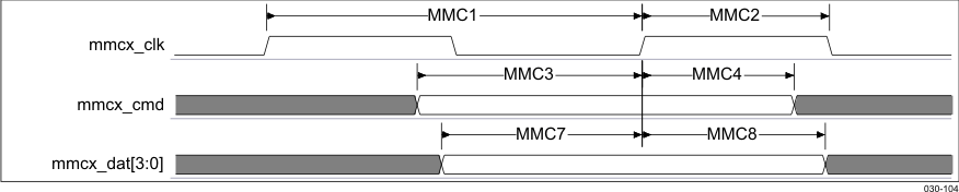
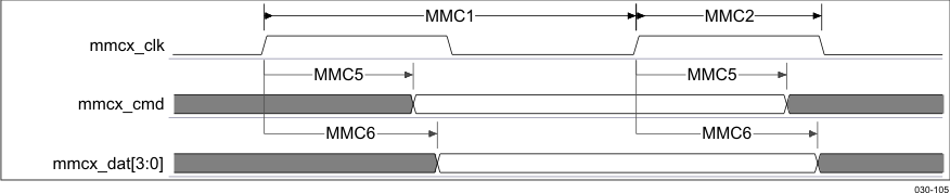
6.7.1.4 MMC/SD/SDIO in High-Speed SD Mode
Table 6-144 through Table 6-146 assume testing over the recommended operating conditions and electrical characteristic conditions.
Table 6-144 MMC/SD/SDIO Timing Conditions High-Speed SD Mode
| TIMING CONDITION PARAMETER | 1.8V, 3.3V | UNIT | ||
|---|---|---|---|---|
| MIN | MAX | |||
| High-Speed SD Mode | ||||
| Input Conditions | ||||
| tR | Input signal rise time | 0.19 | 3 | ns |
| tF | Input signal fall time | 0.19 | 3 | ns |
| Output Conditions | ||||
| CLOAD | Output load capacitance | 30 | pF | |
Table 6-145 MMC/SD/SDIO Timing Requirements High-Speed SD Mode(3)(2)(1)
| NO. | PARAMETER | 1.8V, 3.3V | UNIT | ||
|---|---|---|---|---|---|
| MIN | MAX | ||||
| High-Speed SD Mode | |||||
| MMC/SD/SDIO Interface 1 | |||||
| HSSD3 | tsu(CMDV-CLKIH) | Setup time, mmc1_cmd valid before mmc1_clk rising clock edge | 5.61 | ns | |
| HSSD4 | th(CLKIH-CMDIV) | Hold time, mmc1_cmd valid after mmc1_clk rising clock edge | 2.28 | ns | |
| HSSD7 | tsu(DATxV-CLKIH) | Setup time, mmc1_datx valid before mmc1_clk rising clock edge | 5.61 | ns | |
| HSSD8 | th(CLKIH-DATxIV) | Hold time, mmc1_datx valid after mmc1_clk rising clock edge | 2.28 | ns | |
| MMC/SD/SDIO Interface 2 | |||||
| HSSD3 | tsu(CMDV-CLKIH) | Setup time, mmc2_cmd valid before mmc2_clk rising clock edge | 5.61 | ns | |
| HSSD4 | th(CLKIH-CMDIV) | Hold time, mmc2_cmd valid after mmc2_clk rising clock edge | 2.28 | ns | |
| HSSD7 | tsu(DATxV-CLKIH) | Setup time, mmc2_datx valid before mmc2_clk rising clock edge | 5.61 | ns | |
| HSSD8 | th(CLKIH-DATxIV) | Hold time, mmc2_datx valid after mmc2_clk rising clock edge | 2.28 | ns | |
| MMC/SD/SDIO Interface 3 | |||||
| HSSD3 | tsu(CMDV-CLKIH) | Setup time, mmc3_cmd valid before mmc3_clk rising clock edge | 5.61 | ns | |
| HSSD4 | th(CLKIH-CMDIV) | Hold time, mmc3_cmd valid after mmc3_clk rising clock edge | 2.28 | ns | |
| HSSD7 | tsu(DATxV-CLKIH) | Setup time, mmc3_datx valid before mmc3_clk rising clock edge | 5.61 | ns | |
| HSSD8 | th(CLKIH-DATxIV) | Hold time, mmc3_datx valid after mmc3_clk rising clock edge | 2.28 | ns | |
Table 6-146 MMC/SD/SDIO Switching Characteristics High-Speed SD Mode(3)(2)
| NO. | PARAMETER | 1.8 V, 3.3 V | UNIT | ||
|---|---|---|---|---|---|
| MIN | MAX | ||||
| High-Speed SD Mode | |||||
| HSSD1 | tc(clk) | Cycle time | 20.83 | ns | |
| HSSD2 | tW(clkH) | Typical pulse duration, output clk high | X(4)*PO(1) | ns | |
| HSSD2 | tW(clkL) | Typical pulse duration, output clk low | Y(5)*PO(1) | ns | |
| tdc(clk) | Duty cycle error, output clk | 1041.67 | ps | ||
| tj(clk) | Jitter standard deviation | 200 | ps | ||
| MMC/SD/SDIO Interface 1 | |||||
| tr(clk) | Rise time, output clk | 3 | ns | ||
| tf(clkH) | Fall time, output clk | 3 | ns | ||
| tr(clkL) | Rise time, output data | 3 | ns | ||
| tf(clk) | Fall time, output data | 3 | ns | ||
| HSSD5 | td(CLKOH-CMD) | Delay time, mmc1_clk rising clock edge to mmc1_cmd transition | 3.72 | 14.11 | ns |
| HSSD6 | td(CLKOH-DATx) | Delay time, mmc1_clk rising clock edge to mmc1_datx transition | 3.72 | 14.11 | ns |
| MMC/SD/SDIO Interface 2 | |||||
| tr(clk) | Rise time, output clk | 3 | ns | ||
| tf(clkH) | Fall time, output clk | 3 | ns | ||
| tr(clkL) | Rise time, output data | 3 | ns | ||
| tf(clk) | Fall time, output data | 3 | ns | ||
| HSSD5 | td(CLKOH-CMD) | Delay time, mmc2_clk rising clock edge to mmc2_cmd transition | 3.72 | 14.11 | ns |
| HSSD6 | td(CLKOH-DATx) | Delay time, mmc2_clk rising clock edge to mmc2_datx transition | 3.72 | 14.11 | ns |
| MMC/SD/SDIO Interface 3 | |||||
| tr(clk) | Rise time, output clk | 3 | ns | ||
| tf(clkH) | Fall time, output clk | 3 | ns | ||
| tr(clkL) | Rise time, output data | 3 | ns | ||
| tf(clk) | Fall time, output data | 3 | ns | ||
| HSSD5 | td(CLKOH-CMD) | Delay time, mmc3_clk rising clock edge to mmc3_cmd transition | 3.72 | 14.11 | ns |
| HSSD6 | td(CLKOH-DATx) | Delay time, mmc3_clk rising clock edge to mmc3_datx transition | 3.72 | 14.11 | ns |
Table 6-147 X Parameters
| CLKD | X |
|---|---|
| 1 or Even | 0.5 |
| Odd | (trunc[CLKD/2]+1)/CLKD |
Table 6-148 Y Parameters
| CLKD | Y |
|---|---|
| 1 or Even | 0.5 |
| Odd | (trunc[CLKD/2])/CLKD |
For details about clock division factor CLKD, see the AM35x ARM Microprocessor Technical Reference Manual (SPRUGR0).
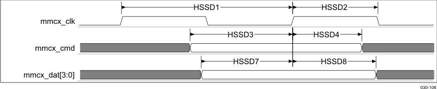
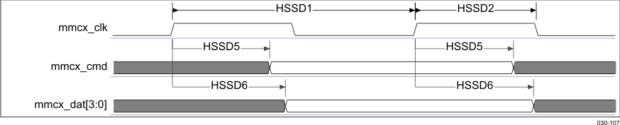
6.7.1.5 MMC/SD/SDIO in Standard SD Mode
Table 6-149 through Table 6-151 assume testing over the recommended operating conditions and electrical characteristic conditions.
Table 6-149 MMC/SD/SDIO Timing Conditions Standard SD Mode
| TIMING CONDITION PARAMETER | 1.8V, 3.3V | UNIT | ||
|---|---|---|---|---|
| MIN | MAX | |||
| Standard SD Mode | ||||
| Input Conditions | ||||
| tR | Input signal rise time | 0.19 | 10 | ns |
| tF | Input signal fall time | 0.19 | 10 | ns |
| Output Conditions | ||||
| CLOAD | Output load capacitance | 30 | pF | |
Table 6-150 MMC/SD/SDIO Timing Requirements Standard SD Mode(1)(2)(3)
| NO. | PARAMETER | 1.8 V, 3.3V | UNIT | ||
|---|---|---|---|---|---|
| MIN | MAX | ||||
| Standard SD Mode | |||||
| MMC/SD/SDIO Interface 1 | |||||
| SD3 | tsu(CMDV-CLKIH) | Setup time, mmc1_cmd valid before mmc1_clk rising clock edge | 6.23 | ns | |
| SD4 | th(CLKIH-CMDIV) | Hold time, mmc1_cmd valid after mmc1_clk rising clock edge | 19.37 | ns | |
| SD7 | tsu(DATxV-CLKIH) | Setup time, mmc1_datx valid before mmc1_clk rising clock edge | 6.23 | ns | |
| SD8 | th(CLKIH-DATxIV) | Hold time, mmc1_datx valid after mmc1_clk rising clock edge | 19.37 | ns | |
| MMC/SD/SDIO Interface 2 | |||||
| SD3 | tsu(CMDV-CLKIH) | Setup time, mmc2_cmd valid before mmc2_clk rising clock edge | 6.23 | ns | |
| SD4 | th(CLKIH-CMDIV) | Hold time, mmc2_cmd valid after mmc2_clk rising clock edge | 19.37 | ns | |
| SD7 | tsu(DATxV-CLKIH) | Setup time, mmc2_datx valid before mmc2_clk rising clock edge | 6.23 | ns | |
| SD8 | th(CLKIH-DATxIV) | Hold time, mmc2_datx valid after mmc2_clk rising clock edge | 19.37 | ns | |
| MMC/SD/SDIO Interface 3 | |||||
| SD3 | tsu(CMDV-CLKIH) | Setup time, mmc3_cmd valid before mmc3_clk rising clock edge | 6.23 | ns | |
| SD4 | th(CLKIH-CMDIV) | Hold time, mmc3_cmd valid after mmc3_clk rising clock edge | 19.37 | ns | |
| SD7 | tsu(DATxV-CLKIH) | Setup time, mmc3_datx valid before mmc3_clk rising clock edge | 6.23 | ns | |
| SD8 | th(CLKIH-DATxIV) | Hold time, mmc3_datx valid after mmc3_clk rising clock edge | 19.37 | ns | |
Table 6-151 MMC/SD/SDIO Switching Characteristics Standard SD Mode(2)(3)
| NO. | PARAMETER | 1.8V, 3.3V | UNIT | ||
|---|---|---|---|---|---|
| MIN | MAX | ||||
| Standard SD Mode | |||||
| SD1 | tc(clk) | Cycle time | 41.67 | ns | |
| SD2 | tW(clkH) | Typical pulse duration, output clk high | X(4)*PO(1) | ns | |
| SD2 | tW(clkL) | Typical pulse duration, output clk low | Y(5)*PO(1) | ns | |
| tdc(clk) | Duty cycle error, output clk | 2083.33 | ps | ||
| tj(clk) | Jitter standard deviation | 200 | ps | ||
| MMC/SD/SDIO Interface 1 | |||||
| tr(clk) | Rise time, output clk | 10 | ns | ||
| tf(clkH) | Fall time, output clk | 10 | ns | ||
| tr(clkL) | Rise time, output data | 10 | ns | ||
| tf(clk) | Fall time, output data | 10 | ns | ||
| SD5 | td(CLKOH-CMD) | Delay time, mmc1_clk rising clock edge to mmc1_cmd transition | 6.13 | 35.53 | ns |
| SD6 | td(CLKOH-DATx) | Delay time, mmc1_clk rising clock edge to mmc1_datx transition | 6.13 | 35.53 | ns |
| MMC/SD/SDIO Interface 2 | |||||
| tr(clk) | Rise time, output clk | 10 | ns | ||
| tf(clkH) | Fall time, output clk | 10 | ns | ||
| tr(clkL) | Rise time, output data | 10 | ns | ||
| tf(clk) | Fall time, output data | 10 | ns | ||
| SD5 | td(CLKOH-CMD) | Delay time, mmc2_clk rising clock edge to mmc2_cmd transition | 6.13 | 35.53 | ns |
| SD6 | td(CLKOH-DATx) | Delay time, mmc2_clk rising clock edge to mmc2_datx transition | 6.13 | 35.53 | ns |
| MMC/SD/SDIO Interface 3 | |||||
| tr(clk) | Rise time, output clk | 10 | ns | ||
| tf(clkH) | Fall time, output clk | 10 | ns | ||
| tr(clkL) | Rise time, output data | 10 | ns | ||
| tf(clk) | Fall time, output data | 10 | ns | ||
| SD5 | td(CLKOH-CMD) | Delay time, mmc3_clk rising clock edge to mmc3_cmd transition | 6.13 | 35.53 | ns |
| SD6 | td(CLKOH-DATx) | Delay time, mmc3_clk rising clock edge to mmc3_datx transition | 6.13 | 35.53 | ns |
Table 6-152 X Parameter
| CLKD | X |
|---|---|
| 1 or Even | 0.5 |
| Odd | (trunc[CLKD/2]+1)/CLKD |
Table 6-153 Y Parameter
| CLKD | Y |
|---|---|
| 1 or Even | 0.5 |
| Odd | (trunc[CLKD/2])/CLKD |
For details about clock division factor CLKD, see the AM35x ARM Microprocessor Technical Reference Manual (SPRUGR0).
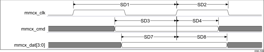
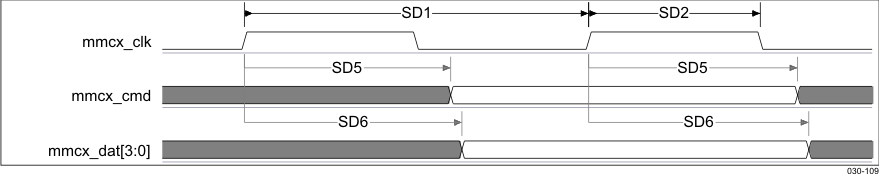
6.8 Test Interfaces
The emulation and trace interfaces allow tracing activities of the following CPUs:
- ARM CortexTM-A8 through an Embedded Trace Macro-cell (ETM11) dedicated to enable real-time trace of the ARM subsystem operations.
All processors can be emulated via JTAG ports.
6.8.1 Embedded Trace Macro Interface (ETM)
Table 6-154 assumes testing over the recommended operating conditions.
Table 6-154 Embedded Trace Macro Interface Switching Characteristics
| NO. | PARAMETER | MIN | MAX | UNIT | |
|---|---|---|---|---|---|
| f | 1/tc(CLK) | Frequency, etk_clk | 166 | MHz | |
| ETM0 | tc(CLK) | Cycle time | 6.02 | ns | |
| ETM1 | tW(CLK) | Clock pulse width, etk_clk | 3.01 | ns | |
| ETM2 | td(CLK-CTL) | Delay time, etk_clk clock edge to etk_ctl transition | -0.5 | 0.5 | ns |
| ETM3 | td(CLK-D) | Delay time, etk_clk clock high to etk_d[15:0] transition | -0.5 | 0.5 | ns |
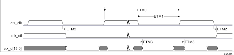 Figure 6-72 Embedded Trace Macro Interface
6.8.2 JTAG Interfaces
AM3517/05 JTAG TAP controller handles standard IEEE JTAG interfaces. The following sections define the timing requirements for several tools used to test the AM3517/05 processors as:
- Free running clock tool, like XDS560 and XDS510 tools
- Adaptive clock tool, like RealView ICE tool and Lauterbach tool
6.8.2.1 JTAG Free Running Clock Mode
Table 6-155 through Table 6-157 assume testing over the recommended operating conditions and electrical characteristic conditions.
Table 6-155 JTAG Timing Conditions Free Running Clock Mode
| TIMING CONDITION PARAMETER | 1.8 V | 3.3 V | UNIT | |
|---|---|---|---|---|
| MAX | MAX | |||
| Input Conditions | ||||
| tR | Input signal rise time | 5 | 3 | ns |
| tF | Input signal fall time | 5 | 3 | ns |
| Output Conditions | ||||
| CLOAD | Output load capacitance | 30 | pF | |
Table 6-156 JTAG Timing Requirements Free Running Clock Mode(1)(2)(3)
| NO. | PARAMETER | 1.8V | 3.3V | UNIT | |||
|---|---|---|---|---|---|---|---|
| MIN | MAX | MIN | MAX | ||||
| JT4 | tc(tck) | Cycle time | 20 | 20 | ns | ||
| JT5 | tw(tckL) | Typical pulse duration, jtag_tck low | 10 | 10 | ns | ||
| JT6 | tw(tckH) | Typical pulse duration, jtag_tck high | 10 | 10 | ns | ||
| tdc(tck) | Duty cycle error, jtag_tck | -1250 | 1250 | -1250 | 1250 | ps | |
| tj(tck) | Cycle jitter | -1250 | 1250 | -1250 | 1250 | ps | |
| JT7 | tsu(tdiV-rtckH) | Setup time, jtag_tdi valid before jtag_rtck high | 1.8 | 3.8 | ns | ||
| JT8 | th(tdiV-rtckH) | Hold time, jtag_tdi valid after jtag_rtck high | 0.7 | 2.7 | ns | ||
| JT9 | tsu(tmsV-rtckH) | Setup time, jtag_tms valid before jtag_rtck high | 1.8 | 3.8 | ns | ||
| JT10 | th(tmsV-rtckH) | Hold time, jtag_tms valid after jtag_rtck high | 0.7 | 2.7 | ns | ||
| JT12 | tsu(emuxV-rtckH) | Setup time, jtag_emux | 14.6 | 14.6 | ns | ||
| JT13 | th(emuxV-rtckH) | Hold time,jtag_emux | 2 | 2 | ns | ||
Table 6-157 JTAG Switching Characteristics Free Running Clock Mode(1)(2)
| 1.8 V | 3.3 V | ||||||
|---|---|---|---|---|---|---|---|
| NO. | PARAMETER | MIN | MAX | MIN | MAX | UNIT | |
| JT1 | tc(rtck) | Cycle time(1), jtag_rtck period | 20 | 20 | ns | ||
| JT2 | tw(rtckL) | Typical pulse duration, jtag_rtck low | 10 | 10 | ns | ||
| JT3 | tw(rtckH) | Typical pulse duration, jtag_rtck high | 10 | 10 | ns | ||
| tdc(rtck) | Duty cycle error, jtag_rtck | -1250 | 1250 | -1250 | 1250 | ps | |
| tj(rtck) | Jitter standard deviation(2), jtag_rtck | 33.33 | 33.33 | ps | |||
| tR(rtck) | Rise time, jtag_rtck | 4 | 4 | ns | |||
| tF(rtck) | Fall time, jtag_rtck | 4 | 4 | ns | |||
| JT11 | td(rtckL-tdoV) | Delay time, jtag_rtck low to jtag_tdo valid | -5.8 | 5.8 | -8 | 8 | ns |
| tR(tdo) | Rise time, jtag_tdo | 4 | 4 | ns | |||
| tF(tdo) | Fall time, jtag_tdo | 4 | 4 | ns | |||
| JT14 | td(rtckH-emuxV) | Delay time, jtag_rtck high to ,jtag_emux | 2.7 | 15.1 | 2.7 | 15.1 | ns |
| tR(emux) | Rise time, jtag_emux | 6 | 6 | ns | |||
| tF(emux) | Fall time, jtag_emux | 6 | 6 | ns | |||
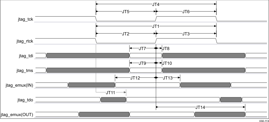
6.8.2.2 JTAG Adaptive Clock Mode
Table 6-158 through Table 6-160 assume testing over the recommended operating conditions and electrical characteristic conditions.
Table 6-158 JTAG Timing Conditions Adaptive Clock Mode
| TIMING CONDITION PARAMETER | 1.8 V | 3.3 V | UNIT | |
|---|---|---|---|---|
| MAX | MAX | |||
| Input Conditions | ||||
| tR | Input signal rise time | 5 | 3 | ns |
| tF | Input signal fall time | 5 | 3 | ns |
| Output Conditions | ||||
| CLOAD | Output load capacitance | 30 | pF | |
Table 6-159 JTAG Timing Requirements Adaptive Clock Mode(1)(2)
| 1.8 V | 3.3 V | ||||||
|---|---|---|---|---|---|---|---|
| NO. | PARAMETER | MIN | MAX | MIN | MAX | UNIT | |
| JA4 | tc(tck) | Cycle time | 20 | 20 | ns | ||
| JA5 | tw(tckL) | Typical pulse duration, jtag_tck low | 10 | 10 | ns | ||
| JA6 | tw(tckH) | Typical pulse duration, jtag_tck high | 10 | 10 | ns | ||
| tdc(lclk) | Duty cycle error, jtag_tck | -2500 | 2500 | -2500 | 2500 | ps | |
| tj(lclk) | Cycle jitter | -1500 | 1500 | -1500 | 1500 | ps | |
| JA7 | tsu(tdiV-tckH) | Setup time, jtag_tdi valid before jtag_tck high | 13.8 | 13.8 | ns | ||
| JA8 | th(tdiV-tckH) | Hold time, jtag_tdi valid after jtag_tck high | 13.8 | 13.8 | ns | ||
| JA9 | tsu(tmsV-tckH) | Setup time, jtag_tms valid before jtag_tck high | 13.8 | 13.8 | ns | ||
| JA10 | th(tmsV-tckH) | Hold time, jtag_tms valid after jtag_tck high | 13.8 | 13.8 | ns | ||
Table 6-160 JTAG Switching Characteristics Adaptive Clock Mode(1)
| 1.8 V | 3.3 V | ||||||
|---|---|---|---|---|---|---|---|
| NO. | PARAMETER | MIN | MAX | MIN | MAX | UNIT | |
| JA1 | tc(rtck) | Cycle time | 20 | 20 | ns | ||
| JA2 | tw(rtckL) | Typical pulse duration, jtag_rtck low | 10 | 10 | ns | ||
| JA3 | tw(rtckH) | Typical pulse duration, jtag_rtck high | 10 | 10 | ns | ||
| tdc(rtck) | Duty cycle error, jtag_rtck | -2500 | 2500 | -2500 | 2500 | ps | |
| tj(rtck) | Jitter standard deviation | 33.33 | 33.33 | ps | |||
| tR(rtck) | Rise time, jtag_rtck | 4 | 4 | ns | |||
| tF(rtck) | Fall time, jtag_rtck | 4 | 4 | ns | |||
| JA11 | td(rtckL-tdoV) | Delay time, jtag_rtck low to jtag_tdo valid | -14.6 | 14.6 | -14.6 | 14.6 | ns |
| tR(tdo) | Rise time, jtag_tdo, | 4 | 4 | ns | |||
| tF(tdo) | Fall time, jtag_tdo | 4 | 4 | ns | |||
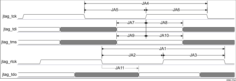 Figure 6-74 JTAG Interface Timing Adaptive Clock Mode