ZHCSCQ1B October 2013 – August 2014 ADS7253 , ADS7853 , ADS8353
PRODUCTION DATA.
- 1 特性
- 2 应用
- 3 说明
- 4 修订历史记录
- 5 Device Comparison Table
- 6 Pin Configurations and Functions
-
7 Specifications
- 7.1 Absolute Maximum Ratings
- 7.2 Handling Ratings
- 7.3 Recommended Operating Conditions
- 7.4 Thermal Information
- 7.5 Electrical Characteristics: ADS8353
- 7.6 Electrical Characteristics: ADS7853
- 7.7 Electrical Characteristics: ADS7253
- 7.8 Electrical Characteristics: All Devices
- 7.9 Timing Requirements: Interface Mode
- 7.10 Timing Characteristics: Serial Interface
- 7.11 Typical Characteristics: ADS8353
- 7.12 Typical Characteristics: ADS7853
- 7.13 Typical Characteristics: ADS7253
- 7.14 Typical Characteristics: Common to ADS8353, ADS7853, and ADS7253
-
8 Detailed Description
- 8.1 Overview
- 8.2 Functional Block Diagram
- 8.3 Feature Description
- 8.4 Device Functional Modes
- 8.5 Register Maps and Serial Interface
- 9 Application and Implementation
- 10Power-Supply Recommendations
- 11Layout
- 12器件和文档支持
- 13机械封装和可订购信息
封装选项
机械数据 (封装 | 引脚)
散热焊盘机械数据 (封装 | 引脚)
- RTE|16
订购信息
7 Specifications
7.1 Absolute Maximum Ratings(1)
over operating free-air temperature range (unless otherwise noted)| MIN | MAX | UNIT | ||
|---|---|---|---|---|
| AVDD to REFGND_x or DVDD to GND | –0.3 | 6 | V | |
| Analog (AINP_x and AINM_x) and reference input (REFIO_x) voltage with respect to REFGND_x | REFGND_x – 0.3 | AVDD + 0.3 | V | |
| Digital input voltage with respect to GND | GND – 0.3 | DVDD + 0.3 | V | |
| Ground voltage difference |REFGND_x-GND| | 0.3 | V | ||
| Input current to any pin except supply pins | ±10 | mA | ||
| Maximum virtual junction temperature, TJ | 150 | °C | ||
(1) Stresses beyond those listed under Absolute Maximum Ratings may cause permanent damage to the device. These are stress ratings only, which do not imply functional operation of the device at these or any other conditions beyond those indicated under Recommended Operating Conditions. Exposure to absolute-maximum-rated conditions for extended periods may affect device reliability.
7.2 Handling Ratings
| MIN | MAX | UNIT | |||
|---|---|---|---|---|---|
| Tstg | Storage temperature range | –65 | 150 | °C | |
| V(ESD) | Electrostatic discharge | Human body model (HBM), per ANSI/ESDA/JEDEC JS-001, all pins(1) | –2000 | 2000 | V |
| Charged device model (CDM), per JEDEC specification JESD22-C101, all pins(2) | –500 | 500 | |||
(1) JEDEC document JEP155 states that 500-V HBM allows safe manufacturing with a standard ESD control process.
(2) JEDEC document JEP157 states that 250-V CDM allows safe manufacturing with a standard ESD control process.
7.3 Recommended Operating Conditions
over operating free-air temperature range (unless otherwise noted)| MIN | NOM | MAX | UNIT | ||
|---|---|---|---|---|---|
| AVDD | Analog supply voltage | 5 | V | ||
| DVDD | Digital supply voltage | 3.3 | V | ||
7.4 Thermal Information
| THERMAL METRIC(1) | ADS8353, ADS7853, ADS7253 | UNIT | ||
|---|---|---|---|---|
| RTE (WQFN) | PW (TSSOP) | |||
| 16 PINS | 16 PINS | |||
| RθJA | Junction-to-ambient thermal resistance | 33.3 | 86.9 | °C/W |
| RθJC(top) | Junction-to-case (top) thermal resistance | 29.5 | 21 | |
| RθJB | Junction-to-board thermal resistance | 7.3 | 39.1 | |
| ψJT | Junction-to-top characterization parameter | 0.2 | 0.8 | |
| ψJB | Junction-to-board characterization parameter | 7.4 | 38.4 | |
| RθJC(bot) | Junction-to-case (bottom) thermal resistance | 0.9 | N/A | |
(1) For more information about traditional and new thermal metrics, see the IC Package Thermal Metrics application report, SPRA953.
7.5 Electrical Characteristics: ADS8353
All minimum and maximum specifications are at TA = –40°C to 125°C, AVDD = 5 V, DVDD = 3.3 V, VREF_A = VREF_B = VREF = 2.5 V (internal), and fDATA = 600 kSPS, unless otherwise noted.Typical values are at TA = 25°C, AVDD = 5 V, and DVDD = 3.3 V.
| PARAMETER | TEST CONDITIONS | MIN | TYP | MAX | UNIT | |
|---|---|---|---|---|---|---|
| RESOLUTION | ||||||
| Resolution | 16 | Bits | ||||
| DC ACCURACY(2) | ||||||
| NMC | No missing codes | 32-clock mode | 16 | Bits | ||
| INL | Integral nonlinearity | 32-clock mode | –2.5 | ±1 | 2.5 | LSB |
| DNL | Differential nonlinearity | 32-clock mode | –0.99 | ±0.6 | 2 | LSB |
| EIO | Input offset error | –1 | ±0.5 | 1 | mV | |
| EIO match | ADC_A to ADC_B | –1 | ±0.5 | 1 | mV | |
| dEIO/dT | Input offset thermal drift | 1 | μV/°C | |||
| EG | Gain error | Referenced to the voltage at REFIO_x | –0.1 | ±0.05 | 0.1 | %FS |
| EG match | ADC_A to ADC_B | –0.1 | ±0.05 | 0.1 | %FS | |
| dEG/dT | Gain error thermal drift | Referenced to the voltage at REFIO_x | 1 | ppm/°C | ||
| AC ACCURACY(1) | ||||||
| SINAD | Signal-to-noise + distortion | VREF = 2.5 V, VREF input range, 32-clock mode |
80.2 | 83 | dB | |
| VREF = 2.5 V, 2 × VREF input range, 32-clock mode |
83.9 | dB | ||||
| VREF = 5 V (external), VREF input range, 32-clock mode |
88.7 | dB | ||||
| SNR | Signal-to-noise ratio | VREF = 2.5 V, VREF input range, 32-clock mode |
80.5 | 83 | dB | |
| VREF = 2.5 V, 2 × VREF input range, 32-clock mode |
84 | dB | ||||
| VREF = 5 V (external), VREF input range, 32-clock mode |
89 | dB | ||||
| THD | Total harmonic distortion | VREF = 2.5 V, VREF input range, 32-clock mode |
–100 | dB | ||
| VREF = 2.5 V, 2 × VREF input range, 32-clock mode |
–100 | dB | ||||
| VREF = 5 V (external), VREF input range, 32-clock mode |
–100 | dB | ||||
| SFDR | Spurious-free dynamic range | VREF = 2.5 V, VREF input range, 32-clock mode |
105 | dB | ||
| VREF = 2.5 V, 2 × VREF input range, 32-clock mode |
105 | dB | ||||
| VREF = 5 V (external), VREF input range, 32-clock mode |
105 | dB | ||||
(1) All ac parameters are tested at –0.5 dBFS and a 2-kHz input frequency.
(2) LSB = least significant bit.
7.6 Electrical Characteristics: ADS7853
All minimum and maximum specifications are at TA = –40°C to 125°C, AVDD = 5 V, DVDD = 3.3 V, VREF_A = VREF_B = VREF = 2.5 V (internal), and fDATA = 1 MSPS, unless otherwise noted.Typical values are at TA = 25°C, AVDD = 5 V, and DVDD = 3.3 V.
| PARAMETER | TEST CONDITIONS | MIN | TYP | MAX | UNIT | ||
|---|---|---|---|---|---|---|---|
| RESOLUTION | |||||||
| Resolution | 14 | Bits | |||||
| DC ACCURACY(2) | |||||||
| NMC | No missing codes | 32-clock mode | 14 | Bits | |||
| 16-clock mode | 13 | Bits | |||||
| INL | Integral nonlinearity | 32-clock mode | –2 | ±0.7 | 2 | LSB | |
| 16-clock mode | –2.5 | ±1 | 2.5 | LSB | |||
| DNL | Differential nonlinearity | 32-clock mode | –0.99 | ±0.5 | 1 | LSB | |
| 16-clock mode | –1 | ±0.9 | 2 | LSB | |||
| EIO | Input offset error | –1 | ±0.5 | 1 | mV | ||
| EIO match | ADC_A to ADC_B | –1 | ±0.5 | 1 | mV | ||
| dEIO/dT | Input offset thermal drift | ±1 | μV/°C | ||||
| EG | Gain error | Referenced to the voltage at REFIO_x | –0.1 | ±0.05 | 0.1 | %FS | |
| EG match | ADC_A to ADC_B | –0.1 | ±0.05 | 0.1 | %FS | ||
| dEG/dT | Gain error thermal drift | Referenced to the voltage at REFIO_x | ±1 | ppm/°C | |||
| AC ACCURACY(1) | |||||||
| SINAD | Signal-to-noise + distortion | VREF = 2.5 V, VREF input range |
32-clock mode | 78.4 | 80.9 | dB | |
| 16-clock mode | 80.3 | dB | |||||
| VREF = 2.5 V, 2 × VREF input range |
32-clock mode | 81.4 | dB | ||||
| 16-clock mode | 80.8 | dB | |||||
| VREF = 5 V (external), VREF input range |
32-clock mode | 83.9 | dB | ||||
| 16-clock mode | 82.9 | dB | |||||
| SNR | Signal-to-noise ratio | VREF = 2.5 V, VREF input range |
32-clock mode | 78.5 | 81 | dB | |
| 16-clock mode | 80.5 | dB | |||||
| VREF = 2.5 V, 2 × VREF input range |
32-clock mode | 81.5 | dB | ||||
| 16-clock mode | 81 | dB | |||||
| VREF = 5 V (external), VREF input range |
32-clock mode | 84 | dB | ||||
| 16-clock mode | 83.5 | dB | |||||
| THD | Total harmonic distortion | VREF = 2.5 V, VREF input range |
32-clock mode | –100 | dB | ||
| 16-clock mode | –93 | dB | |||||
| VREF = 2.5 V, 2 × VREF input range |
32-clock mode | –98 | dB | ||||
| 16-clock mode | –94 | dB | |||||
| VREF = 5 V (external), VREF input range |
32-clock mode | –102 | dB | ||||
| 16-clock mode | –92 | dB | |||||
| SFDR | Spurious-free dynamic range | VREF = 2.5 V, VREF input range |
32-clock mode | 100 | dB | ||
| 16-clock mode | 95 | dB | |||||
| VREF = 2.5 V, 2 × VREF input range |
32-clock mode | 100 | dB | ||||
| 16-clock mode | 95 | dB | |||||
| VREF = 5 V (external), VREF input range |
32-clock mode | 102 | dB | ||||
| 16-clock mode | 95 | dB | |||||
| ISOXT | ADC-to-ADC isolation | fIN = 15 kHz at 10 %FS, fNOISE = 25 kHz at FS |
–100 | dB | |||
(1) All ac parameters are tested at –0.5 dBFS and a 2-kHz input frequency.
(2) LSB = least significant bit.
7.7 Electrical Characteristics: ADS7253
All minimum and maximum specifications are at TA = –40°C to 125°C, AVDD = 5 V, DVDD = 3.3 V, VREF_A = VREF_B = VREF = 2.5 V (internal), and fDATA = 1 MSPS, unless otherwise noted.Typical values are at TA = 25°C, AVDD = 5 V, and DVDD = 3.3 V.
| PARAMETER | TEST CONDITIONS | MIN | TYP | MAX | UNIT | ||
|---|---|---|---|---|---|---|---|
| RESOLUTION | |||||||
| Resolution | 12 | Bits | |||||
| DC ACCURACY(2) | |||||||
| NMC | No missing codes | 12 | Bits | ||||
| INL | Integral nonlinearity | –1 | ±0.3 | 1 | LSB | ||
| DNL | Differential nonlinearity | –0.99 | ±0.3 | 1 | LSB | ||
| EIO | Input offset error | –2 | ±0.5 | 2 | mV | ||
| EIO match | ADC_A to ADC_B | –2 | ±0.5 | 2 | mV | ||
| dEIO/dT | Input offset thermal drift | ±1 | μV/°C | ||||
| EG | Gain error | Referenced to the voltage at REFIO_x | –0.2 | ±0.05 | 0.2 | %FS | |
| EG match | ADC_A to ADC_B | –0.2 | ±0.05 | 0.2 | %FS | ||
| dEG/dT | Gain error thermal drift | Referenced to the voltage at REFIO_x | ±1 | ppm/°C | |||
| AC ACCURACY(1) | |||||||
| SINAD | Signal-to-noise + distortion | VREF = 2.5 V, VREF input range |
71 | 72.9 | dB | ||
| VREF = 2.5 V, 2 × VREF input range |
72.9 | dB | |||||
| VREF = 5 V (external), VREF input range |
73.4 | dB | |||||
| SNR | Signal-to-noise ratio | VREF = 2.5 V, VREF input range |
71.5 | 73 | dB | ||
| VREF = 2.5 V, 2 × VREF input range |
73 | dB | |||||
| VREF = 5 V (external), VREF input range |
73.5 | dB | |||||
| THD | Total harmonic distortion | VREF = 2.5 V, VREF input range |
–90 | dB | |||
| VREF = 2.5 V, 2 × VREF input range |
–90 | dB | |||||
| VREF = 5 V (external), VREF input range |
–90 | dB | |||||
| SFDR | Spurious-free dynamic range | VREF = 2.5 V, VREF input range |
93.5 | dB | |||
| VREF = 2.5 V, 2 × VREF input range |
93.5 | dB | |||||
| VREF = 5 V (external), VREF input range |
93.5 | dB | |||||
| ISOXT | ADC-to-ADC isolation | fIN = 15 kHz at 10 %FS, fNOISE = 25 kHz at FS |
–80 | dB | |||
(1) All ac parameters are tested at –0.5 dBFS and a 2-kHz input frequency.
(2) LSB = least significant bit.
7.8 Electrical Characteristics: All Devices
All minimum and maximum specifications are at TA = –40°C to 125°C, AVDD = 5 V, DVDD = 3.3 V, VREF_A = VREF_B = VREF = 2.5 V, and fDATA = maximum, unless otherwise noted.Typical values are at TA = 25°C, AVDD = 5 V, and DVDD = 3.3 V.
| PARAMETER | TEST CONDITIONS | MIN | TYP | MAX | UNIT | ||
|---|---|---|---|---|---|---|---|
| ANALOG INPUT | |||||||
| FSR | Full-scale input range(1)
(AINP_x – AINM_x) |
VREF range | Single-ended input, AINM_x = GND |
0 | VREF | V | |
| Pseudo-differential input, AINM_x = +VREF / 2 |
–VREF / 2 | VREF / 2 | V | ||||
| 2 × VREF range | Single-ended input, AINM_x = GND, AVDD ≥ 2 × VREF |
0 | 2 × VREF | V | |||
| Pseudo-differential input, AINM_x = +VREF, AVDD ≥ 2 × VREF |
–VREF | VREF | V | ||||
| VINP | Absolute input voltage (AINP_x to REFGND) |
VREF range | 0 | VREF | V | ||
| 2 × VREF range, AVDD ≥ 2 × VREF | 0 | 2 × VREF | V | ||||
| VINM | Absolute input voltage (AINM_x to REFGND) |
VREF range | Single-ended input | –0.1 | 0.1 | V | |
| Pseudo-differential input | VREF / 2 – 0.1 | VREF / 2 | VREF / 2 + 0.1 | V | |||
| 2 × VREF range | Single-ended input, AVDD ≥ 2 × VREF | –0.1 | 0.1 | V | |||
| Pseudo-differential input, AVDD ≥ 2 × VREF | VREF – 0.1 | VREF | VREF + 0.1 | V | |||
| Ci | Input capacitance | In sample mode | 40 | pF | |||
| In hold mode | 4 | pF | |||||
| Ilkg(i) | Input leakage current | 0.1 | µA | ||||
| INTERNAL VOLTAGE REFERENCE | |||||||
| VREFOUT | Reference output voltage | REFDAC_x = 1FFh (default), at 25°C |
2.495 | 2.500 | 2.505 | V | |
| VREF-match | VREF_A to VREF_B matching | REFDAC_x = 1FFh (default), at 25°C |
±1 | mV | |||
| REFDAC_x resolution(4) | 1.1 | mV | |||||
| dVREFOUT/dT | Reference voltage temperature drift | REFDAC_x = 1FFh (default) | ±10 | ppm/°C | |||
| dVREFOUT/dt | Long-term stability | 1000 hours | 150 | ppm | |||
| RO | Internal reference output impedance | 1 | Ω | ||||
| IREFOUT | Reference output dc current | 2 | mA | ||||
| CREFOUT | Recommended output capacitor | 10 | µF | ||||
| tREFON | Reference output settling time | For CREF = 10 μF | 8 | ms | |||
| VOLTAGE REFERENCE INPUT | |||||||
| VREF | Reference voltage (input) | VREF range | 2.4 | 2.5 | AVDD | V | |
| 2 × VREF range | 2.4 | 2.5 | AVDD / 2 | V | |||
| IREF | Average Reference input current | Per ADC | 300 | μA | |||
| CREF | External ceramic reference capacitance | 10 | μF | ||||
| Ilkg(dc) | DC leakage current | ±0.1 | μA | ||||
| SAMPLING DYNAMICS | |||||||
| tA | Aperture delay | 8 | ns | ||||
| tA match | ADC_A to ADC_B | 40 | ps | ||||
| tAJIT | Aperture jitter | 50 | ps | ||||
| DIGITAL INPUTS(2) | |||||||
| VIH | High-level input voltage | DVDD > 2.3 V | 0.7 DVDD | DVDD + 0.3 | V | ||
| DVDD ≤ 2.3 V | 0.8 DVDD | DVDD + 0.3 | V | ||||
| VIL | Low-level input voltage | DVDD > 2.3 V | –0.3 | 0.3 DVDD | V | ||
| DVDD ≤ 2.3 V | –0.3 | 0.2 DVDD | V | ||||
| Input current | ±10 | nA | |||||
| DIGITAL OUTPUTS(2) | |||||||
| VOH | High-level output voltage | IOH = 500-µA source | 0.8 DVDD | DVDD | V | ||
| VOL | Low-level output voltage | IOH = 500-µA sink | 0 | 0.2 DVDD | V | ||
| POWER SUPPLY | |||||||
| AVDD | Analog supply voltage (AVDD to AGND) |
±VREF range | Internal reference | 4.5 | 5.0 | 5.5 | V |
| External reference: VEXT_REF < 4.5 V | 4.5 | 5.0 | 5.5 | V | |||
| External reference: VEXT_REF > 4.5 V | VEXT_REF | 5.0 | 5.5 | V | |||
| ±2 × VREF range | Internal reference | 5.0 | 5.0 | 5.5 | V | ||
| External reference | 2 × VREF_EXT | 5.0 | 5.5 | V | |||
| DVDD | Digital supply voltage (DVDD to AGND) |
1.65 | 5.5 | V | |||
| AIDD | Analog supply current | AVDD = 5 V, fastest throughput internal reference |
8.5 | 10 | mA | ||
| AVDD = 5 V, fastest throughput external reference(3) |
7.5 | mA | |||||
| AVDD = 5 V, no conversion internal reference |
5.5 | 7 | mA | ||||
| AVDD = 5 V, no conversion external reference(3) |
4.5 | mA | |||||
| AVDD = 5 V, STANDBY mode Internal Reference |
2.5 | mA | |||||
| AVDD = 5 V, STANDBY mode external reference(3) |
1 | mA | |||||
| Power-down mode | 10 | 50 | μA | ||||
| DIDD | Digital supply current | DVDD = 3.3 V, CLOAD = 10 pF, fastest throughput |
0.5 | mA | |||
| DVDD = 5 V, CLOAD = 10 pF fastest throughput |
1 | mA | |||||
| PD | Power dissipation (normal operation) |
AVDD = 5V, fastest throughput, internal reference |
42.5 | 50 | mW | ||
(1) Ideal input span, does not include gain or offset error.
(2) Specified by design; not production tested.
(3) With internal reference powered down, CFR.B6 = 0.
(4) Refer to the Reference section for more details.
7.9 Timing Requirements: Interface Mode(1)
| PARAMETER | ASSOCIATED FIGURES | |
|---|---|---|
| tCLK | CLOCK period | Figure 1, Figure 91, Figure 92, Figure 93, Figure 94 |
| tACQ | Acquisition time | Figure 91, Figure 92, Figure 93, Figure 94 |
| tCONV | Conversion time | Figure 91, Figure 92, Figure 93, Figure 94 |
(1) These parameters are specific to the interface mode of operation. Refer to the Conversion Data Read section for more details.
7.10 Timing Characteristics: Serial Interface
| PARAMETER | TEST CONDITIONS | ASSOCIATED FIGURES | MIN | TYP | MAX | UNIT | ||
|---|---|---|---|---|---|---|---|---|
| TIMING REQUIREMENTS | ||||||||
| tPH_CK | CLOCK high time | Figure 1 | 0.4 | 0.6 | tCLK | |||
| tPL_CK | CLOCK low time | 0.4 | 0.6 | tCLK | ||||
| fCLK | CLOCK frequency | 1 / tCLK | MHz | |||||
| tPH_CS | CS high time | Figure 1 | 40 | ns | ||||
| tPH_CS_SHRT | CS high time after frame abort | ADS8353 | Figure 99 | 150 | ns | |||
| ADS7853 | 100 | ns | ||||||
| ADS7253 | 70 | ns | ||||||
| tSU_CSCK | Setup time: CS falling edge to SCLK falling edge | Figure 1 | 15 | ns | ||||
| tD_CKCS | Delay time: Last SCLK falling edge to CS rising edge | 15 | ns | |||||
| tSU_CKDI | Setup time: DIN data valid to SCLK falling edge | 5 | ns | |||||
| tHT_CKDI | Hold time: SCLK falling edge to (previous) data valid on DIN | 5 | ns | |||||
| tPU_STDBY | Power-up time from STANDBY mode | Figure 96 | 1 | µs | ||||
| tPU_SPD | Power-up time from SPD mode | With internal reference | Figure 98 | 3 | ms | |||
| With external reference | 1 | ms | ||||||
| TIMING SPECIFICATIONS | ||||||||
| tTHROUGHPUT | Throughput time | ADS8353 | 32-CLK mode | Figure 91, Figure 92 | 1.666 | µs | ||
| ADS7853 | 32-CLK mode | 1 | µs | |||||
| 16-CLK mode | Figure 93, Figure 94 | 1 | µs | |||||
| ADS7253 | 32-CLK mode | Figure 91, Figure 92 | 1 | µs | ||||
| 16-CLK mode | Figure 93, Figure 94 | 1 | µs | |||||
| fTHROUGHPUT | Throughput | Figure 91, Figure 92, Figure 93, Figure 94 | 1 / tTHROUGHPUT | kSPS | ||||
| tDV_CSDO | Delay time: CS falling edge to data enable | Figure 1 | 12 | ns | ||||
| tDZ_CSDO | Delay time: CS rising edge to data going to 3-state | 12 | ns | |||||
| tD_CKDO | Delay time: SCLK falling edge to next data valid | 20 | ns | |||||
Figure 1 shows the details of the serial interface between the device and the digital host controller.
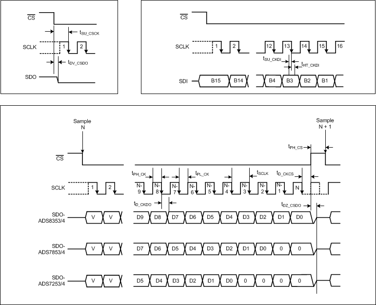 Figure 1. Serial Interface Timing Diagram
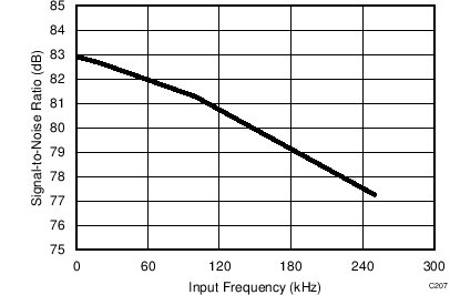
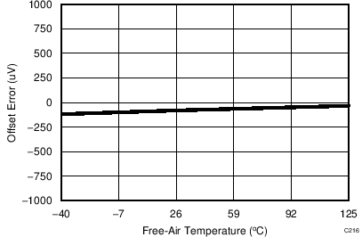
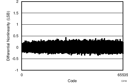
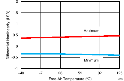
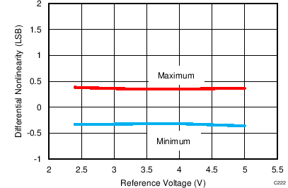
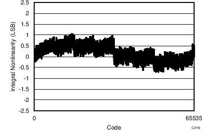
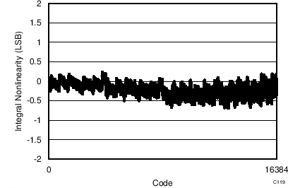
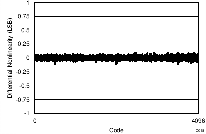
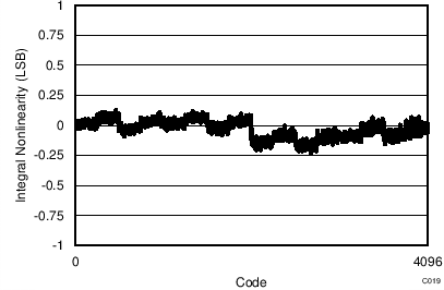
7.11 Typical Characteristics: ADS8353
At TA = 25°C, AVDD = 5 V, DVDD = 3.3 V, VREF = 2.5 V (internal), and fDATA = 600 kSPS, unless otherwise noted.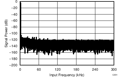
| fIN = 2 kHz | SNR = 84.2 dB | THD = -101.3 dB |
| fIN = 2 kHz |
| fIN = 2 kHz |
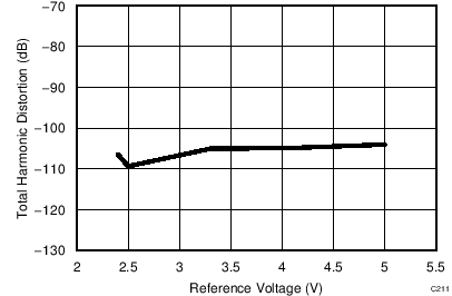
| VREF = 5 V |
| fIN = 2 kHz |
| VREF = 5 V |
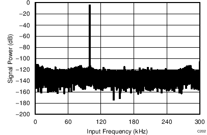
| fIN = 100 kHz | SNR = 80.8 dB | THD = -99.1 dB |
| fIN = 2 kHz |
| fIN = 2 kHz |
| VREF = 5 V |
| fIN = 2 kHz |
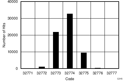
| 65536 data points | VIN-DIFF = 0 V |
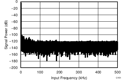
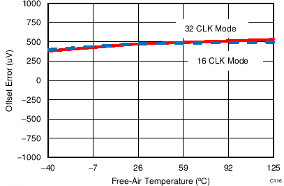
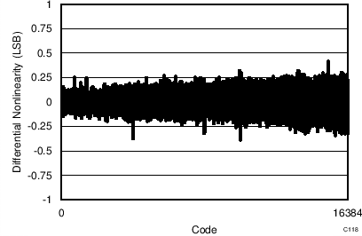
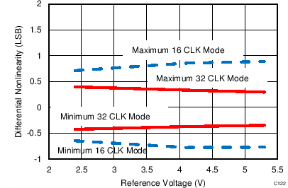
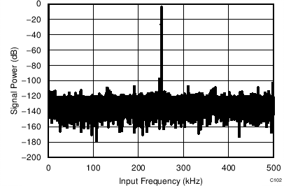
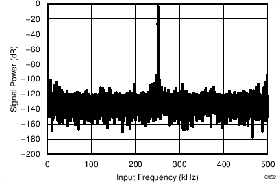
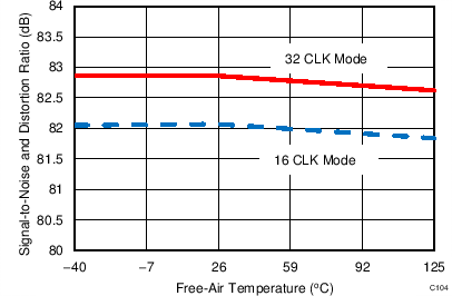
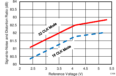
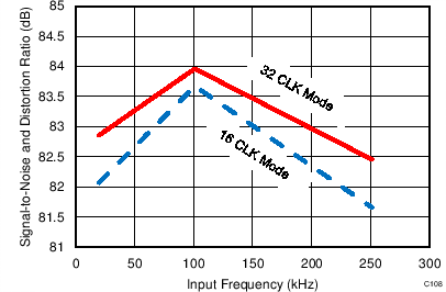
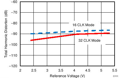
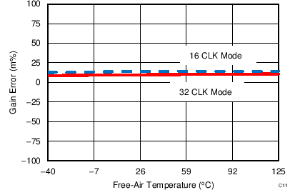
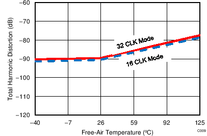
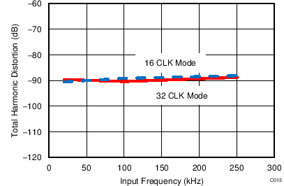
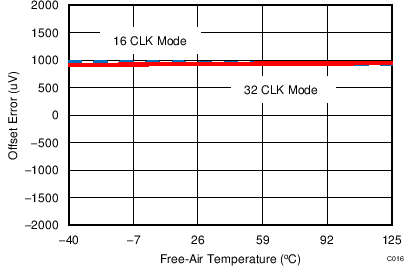
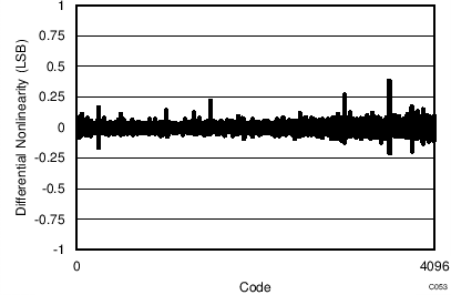
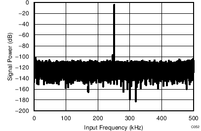
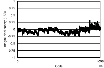
7.12 Typical Characteristics: ADS7853
At TA = 25°C, AVDD = 5 V, DVDD = 3.3 V, VREF = 2.5 V (internal), and fDATA = 1 MSPS, unless otherwise noted.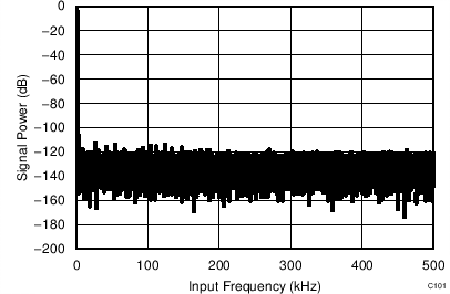
| fIN = 2 kHz | SNR = 81.1 dB | THD = –94.2 dB |
| 16-CLK interface |
| fIN = 2 kHz | SNR = 81.9 dB | THD = –98.1 dB |
| 32-CLK interface |
| fIN = 2 kHz |
| fIN = 2 kHz |
| VREF = 5 V |
| fIN = 2 kHz |
| VREF = 5 V |
| 16-CLK interface |
| 16-CLK interface | 65536 data points | VIN-DIFF = 0 V |
| 16-CLK interface |
| 32-CLK interface |
| fIN = 250 kHz | SNR = 80.2 dB | THD = –90.4 dB |
| 16-CLK interface |
| fIN = 250 kHz | SNR = 80.8 dB | THD = –92.1 dB |
| 32-CLK interface |
| fIN = 2 kHz |
| fIN = 2 kHz |
| VREF = 5 V |
| fIN = 2 kHz |
| 32-CLK interface |
| 32-CLK interface | 65536 data points | VIN-DIFF = 0 V |
| 16-CLK interface |
| 32-CLK interface |
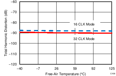
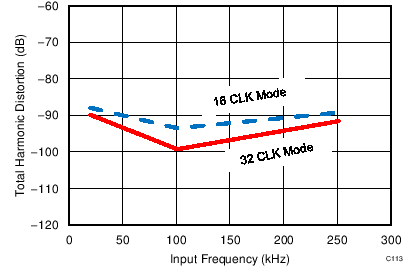
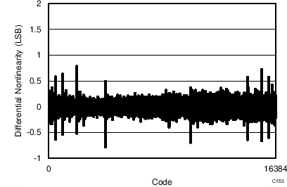
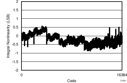
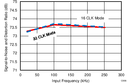
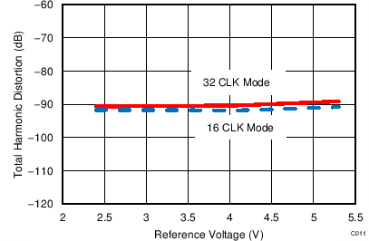
7.13 Typical Characteristics: ADS7253
At TA = 25°C, AVDD = 5 V, DVDD = 3.3 V, VREF = 2.5 V (internal), and fDATA = 1 MSPS, unless otherwise noted.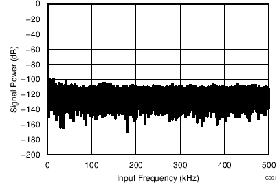
| fIN = 2 kHz | SNR = 73.2 dB | THD = –90.5 dB |
| 16-CLK interface |
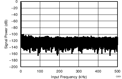
| fIN = 2 kHz | SNR = 73.6 dB | THD = –91.6 dB |
| 32-CLK interface |
| fIN = 2 kHz |
| fIN = 2 kHz |
| VREF = 5 V |
| fIN = 2 kHz |
| VREF = 5 V |
| 16-CLK interface |
| 16-CLK interface | 65536 data points | VIN-DIFF = 0 V |
| 16-CLK interface |
| 32-CLK interface |
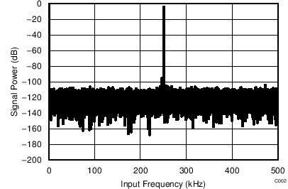
| fIN = 250 kHz | SNR = 73.1 dB | THD = –90.1 dB |
| 16-CLK interface |
| fIN = 250 kHz | SNR = 73.4 dB | THD = –90.6 dB |
| 32-CLK interface |
| fIN = 2 kHz |
| fIN = 2 kHz |
| VREF = 5 V |
| fIN = 2 kHz |
| 32-CLK interface |
| 32-CLK interface | 65536 data points | VIN-DIFF = 0 V |
| 16-CLK interface |
| 32-CLK interface |
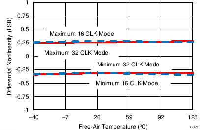
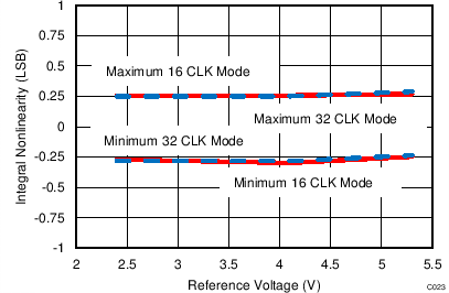
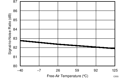
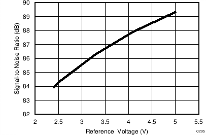
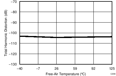
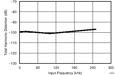
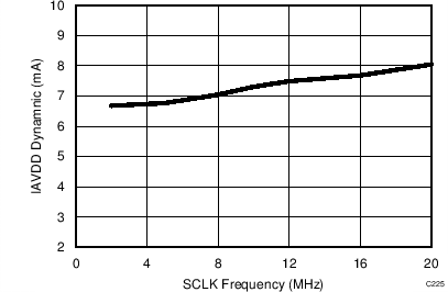
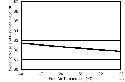
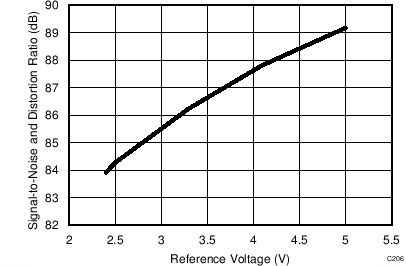
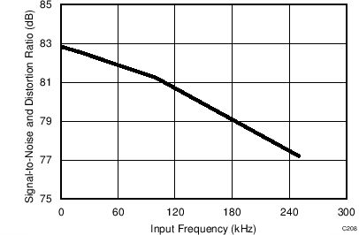
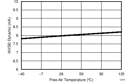
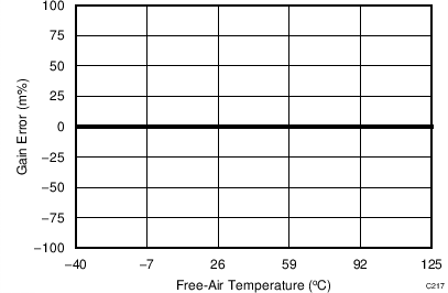
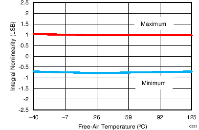
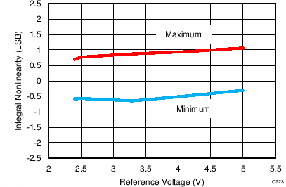
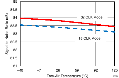
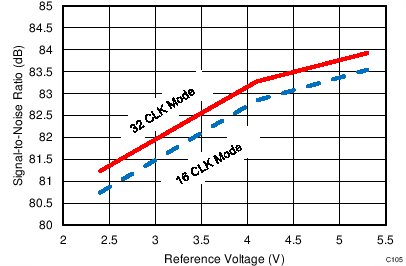
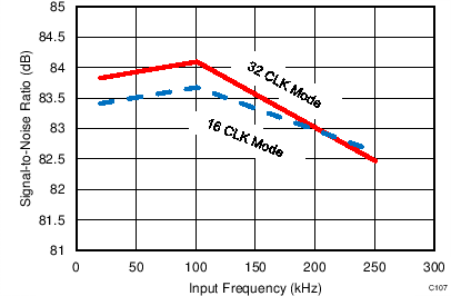
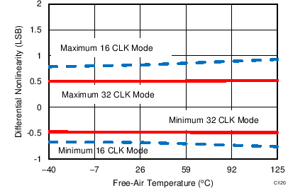
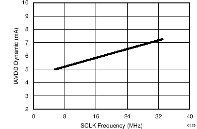
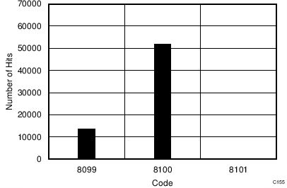
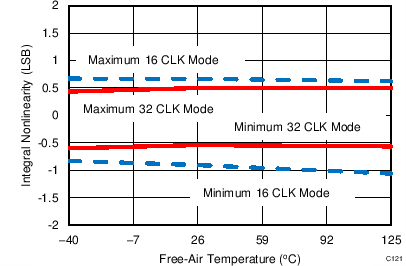
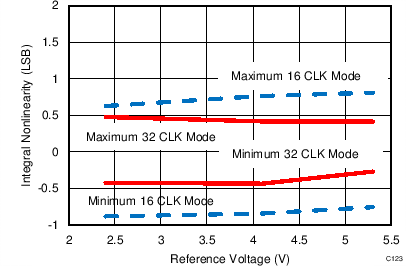
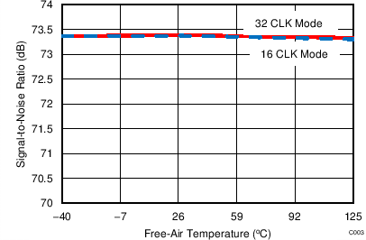
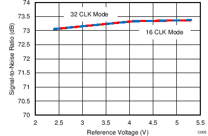
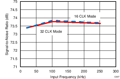
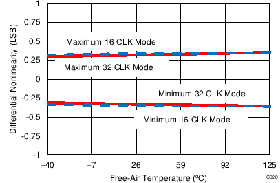
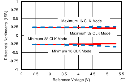
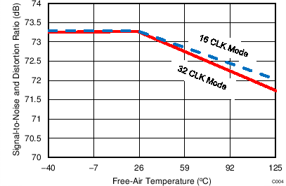
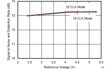
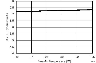
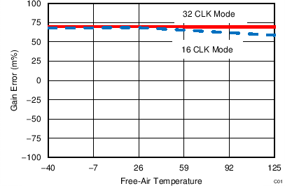
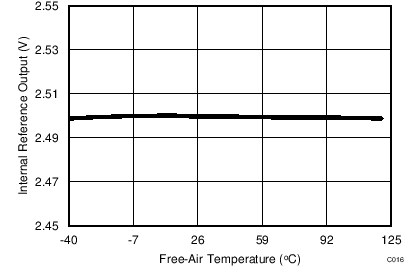
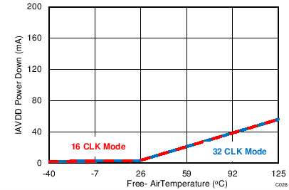
7.14 Typical Characteristics: Common to ADS8353, ADS7853, and ADS7253
At TA = 25°C, AVDD = 5 V, DVDD = 3.3 V, VREF = 2.5 V (internal), and fDATA = maximum, unless otherwise noted.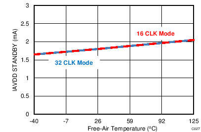
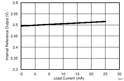
| ROUT = 0.67 Ω |