SLPS482B December 2013 – January 2015 CSD19533KCS
PRODUCTION DATA.
- 1Features
- 2Applications
- 3Description
- 4Revision History
- 5Specifications
- 6Device and Documentation Support
- 7Mechanical, Packaging, and Orderable Information
Package Options
Refer to the PDF data sheet for device specific package drawings
Mechanical Data (Package|Pins)
- KCS|3
Thermal pad, mechanical data (Package|Pins)
Orderable Information
1 Features
- Ultra-Low Qg and Qgd
- Low Thermal Resistance
- Avalanche Rated
- Pb Free Terminal Plating
- RoHS Compliant
- Halogen Free
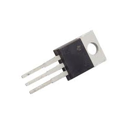
- TO-220 Plastic Package
2 Applications
- Secondary Side Synchronous Rectifier
- Motor Control
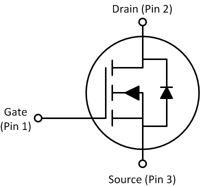
3 Description
This 100 V, 8.7 mΩ, TO-220 NexFET™ power MOSFET is designed to minimize losses in power conversion applications.
Product Summary
| TA = 25°C | TYPICAL VALUE | UNIT | ||
|---|---|---|---|---|
| VDS | Drain-to-Source Voltage | 100 | V | |
| Qg | Gate Charge Total (10 V) | 27 | nC | |
| Qgd | Gate Charge Gate-to-Drain | 5.4 | nC | |
| RDS(on) | Drain-to-Source On-Resistance | VGS = 6 V | 9.7 | mΩ |
| VGS = 10 V | 8.7 | mΩ | ||
| VGS(th) | Threshold Voltage | 2.8 | V | |
Ordering Information(1)
| Device | Package | Media | Qty | Ship |
|---|---|---|---|---|
| CSD19533KCS | TO-220 Plastic Package | Tube | 50 | Tube |
- For all available packages, see the orderable addendum at the end of the data sheet.
Absolute Maximum Ratings
| TA = 25°C | VALUE | UNIT | |
|---|---|---|---|
| VDS | Drain-to-Source Voltage | 100 | V |
| VGS | Gate-to-Source Voltage | ±20 | V |
| ID | Continuous Drain Current (Package limited) | 100 | A |
| Continuous Drain Current (Silicon limited), TC = 25°C | 86 | ||
| Continuous Drain Current (Silicon limited), TC = 100°C | 61 | ||
| IDM | Pulsed Drain Current (1) | 207 | A |
| PD | Power Dissipation | 188 | W |
| TJ, Tstg |
Operating Junction and Storage Temperature Range |
–55 to 175 | °C |
| EAS | Avalanche Energy, single pulse ID = 46 A, L = 0.1 mH, RG = 25 Ω |
106 | mJ |
RDS(on) vs VGS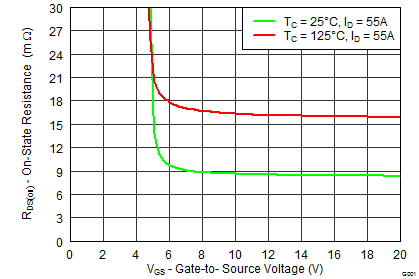 |
Gate Charge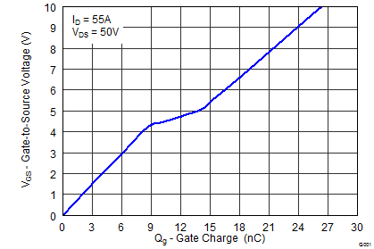 |